A while back I made a prototype of a Commodore 64 PLA replacement chip in FPGA and covered this extensively in this blog post.
You can also choose to watch the video.
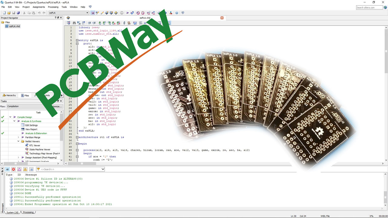
Recently I designed a PCB and thought that it was a good opportunity to describe the whole creation process from scratch. So if you are interested in how something like this comes about or maybe are thinking of creating a similar project yourself, then read on.
This project is sponsored by PCBWay which kindly offered to create PCBs for this project.
But let's start from the beginning and tell you the reason why I even wanted to create another PLA replacement chip in the first place.
When I got this Commodore 64 it was in a non-working condition. The PLA chip was broken. I could have ordered a replacement, but during that time I was also playing around with FPGA development and had a couple of these programmable Altera chips, so I thought to give it a try and create a PLA replacement myself.
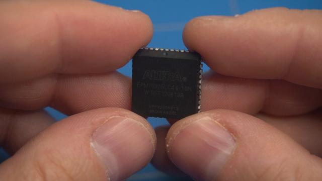
The chip that I have used is this Altera EPM7032. It utilizes a PLCC44 socket, which is easy to solder and friendly to create prototypes.
It's a CPLD chip and it basically works the same as an FPGA chip but has a small advantage in that it can store the contents in non-volatile memory. So when you turn it off, it will not be erased. In an FPGA chip, you usually need to use an external flash chip to accomplish that.
Altera, which by the way was acquired by Intel in 2015, offers a free version of the development environment called Quartus Lite where you can program the chips in Hardware description languages like VHDL or Verilog. To create the PLA replacement chip we will be using VHDL.
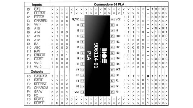
PLA stands for Programmable Logic Array and originally it was based on a Signetics 82S100 chip with 16 inputs and 8 outputs, which could be programmed with the desired logic. It functions as a Traffic Center for communication between all the chips inside the Commodore 64.
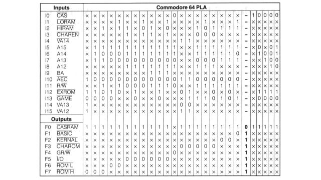
This logic of the PLA chip can be represented with a truth table. Where given inputs always trigger specific outputs.
When we look at this table inside the Transactor Magazine from March 1986 and examine a useful example we see that inside this column the address bus A15 contains a 1, A14 a 0 and A13 a 1, which means that an address in the range of $A000 and $BFFF (hexadecimal) is placed by the microprocessor on the bus. In the output section, we see that the BASIC output is pulled LOW, which means that the BASIC chip will be enabled.
There is also another case when the same address is used, this can happen when a game cartridge of 16 Kilobytes is inserted into the C64. In that case, the GAME and EXROM inputs are pulled LOW. And when that happens the BASIC chip will not be enabled and instead, the memory inside the cartridge will get addressed.
If you are interested in how cartridges work, you can also read the blog post where I build cartridges on a breadboard.
The next step will be to make a translation from the truth table to boolean logic. For this, we can use a method called the sum of products. Let me briefly show how this works based on a simple example of an XOR gate.
This is what the truth table of this gate looks like.
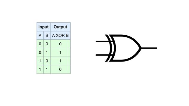
If we look at the output, then it is TRUE in the case when input A is TRUE and input B is FALSE or when A is FALSE and B is TRUE. The other cases produce FALSE output. To define the sum of products for this gate we only need to look at the cases where the output is TRUE. So this happens exactly as we have mentioned before.
OUTPUT = (A AND NOT B) OR (NOT A AND B)
This is enough information for a logic chip like an FPGA to make an XOR gate.
The PLA chip is a bit more complex and has multiple outputs and the outputs can have 3 states. TRUE, FALSE, but also a high impedance state, which does not output anything. In this case, we also need to look at when the output will be FALSE or TRUE.
When we look at the output of ROMH, the output is FALSE when AEC, EXROM, VA13 and VA12 inputs are set to TRUE and also when the GAME input is set to FALSE.
But it is also the case when the conditions of the other two rows apply.
The condition can be written like this. Note that the NOT in front of this statement indicates that the output will be FALSE.
ROMH = NOT (va13 and va12 and aec and exrom and not game
OR a15 and a14 and a13 and not aec and exrom and not game
OR  hiram and a15 and not a14 and a13 and not aec and rd and not exrom and not game)
After gaining these insights we can try to recreate this logic of the PLA inside the Altera CPLD chip using the VHDL language.
We will need an older version of Quartus II Web edition, as it needs to support the family of MAX 7000 chips. The newer versions do not support it. An account on the Intel website is also required before downloading the software. The best is to get the combined files bundle as this will allow you to install everything in one go.

After starting the application we can create a new project using the New Project Wizard.
The first page gives some introduction, we can skip that. On this page, we can select a directory for the project. I will choose this location (C:\Projects\Quartus\ezPLA) and the name of the project, which will be ezPLA.
In the next step, we can add files to the project, but we have none yet. So press next.
This page is important as we can choose the chip that we will be using. It is from the MAX7000S family and the name is EPM7032SLC44-10. We click next and use the defaults here and press Finish.
When we click on File->New there is an option to create an empty VHDL file.
At this point, we could write the whole code from scratch, but let's look for some help. When we search on c64 pla vhdl github keywords, then one of the first hits is the github page of Frank Buss. There we can find a repository that includes the VHDL code for the PLA chip.
Let's copy the raw file into Quartus, save it and walk through the file to see how it works.
On top of the file, there are some headers that will allow us to use boolean logic inside this VHDL file. The inputs and outputs of the chip are defined inside the entity declaration.
entity c64pla7 is
    port(
        a13: in std_logic;
        a14: in std_logic;
        a15: in std_logic;
        va14: in std_logic;
        charen: in std_logic;
        hiram: in std_logic;
        loram: in std_logic;
        cas: in std_logic;
        romh: out std_logic;
        roml: out std_logic;
        io: out std_logic;
        grw: out std_logic;
        charom: out std_logic;
        kernal: out std_logic;
        basic: out std_logic;
        casram: out std_logic;
        xoe: in std_logic;
        va12: in std_logic;
        va13: in std_logic;
        game: in std_logic;
        exrom: in std_logic;
        rw: in std_logic;
        aec: in std_logic;
        ba: in std_logic;
        a12: in std_logic
    );
end c64pla7;
If we look at the pinout of the PLA chip, we can see that it matches this.
The next step is to define how inputs and outputs relate to each other. This is described in the architecture.
architecture rtl of c64pla7 is
The arguments of the process function are the input pins of the chip. In VHDL terms, this is called the sensitivity list.
process(a13, a14, a15, va14, charen, hiram, loram, cas, xoe, va12, va13, game, exrom, rw, aec, ba, a12)
There are 2 states that the chip can be in. The first one is when all of its outputs are in a high impedance state. This happens when the Output Enable (xoe variable) is HIGH. When Output Enable input goes LOW then the second state is enabled and the output pins will be set according to the defined inputs. We have learned before how this logic comes about, we can now investigate how it is written in VHDL.
if xoe = '1' then
   ...
else
   ...
end if;
The ROMH output is LOW when the 3 conditions that we spoke about before are met. There is actually a small mistake in this VHDL code. Let me explain.
The first line refers to this column of the truth table. We see here that the inputs hiram, a15, a13 and rw should be HIGH, and A14, AEC, EXROM and GAME are expected to be LOW. However, the AEC is reversed here. I am not sure about the reason for that, but it's throughout the whole code.
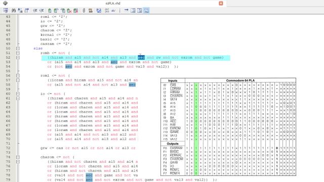
The second and third lines in the code match these 2 columns of the truth table. All these conditions are glued together using the OR statement, and the NOT in front of all of them means that ROMH will be set to a logical 0 when any of these 3 lines are true.
The same is done to the other outputs. The last line for the CASRAM output is the longest as it needs to cover all of these cases here.
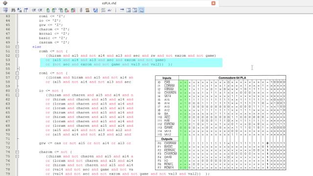
First, let's invert all of the AEC values inside the code. I will do that by first replacing all the not aec to a TOKEN string, then the string aec to not aec. And finally the string TOKEN to aec.
Next, we will need to assign the inputs and outputs of this VHDL entity to real pins on the chip.
This can be done by clicking on the Pin Planner icon in the toolbar. At this point, the list is empty as the application does not know what the inputs and outputs are. We need to compile the code first.
And we got an error. Ah.. the replacement of the AEC string did not need to put "not" in front of this AEC pin definition on this line. Let's change it back and also do it on this line. The rest should be fine.
How about another try compiling this thing. And we got another error. What is it now? Oh.. ezPLA is undefined. Apparently, the VHDL code expects that the name of the file should be the same as of the entity. Ok. Let's change the c64pla7 to ezPLA and give it another try...
This time it's a success. We can ignore the warnings.
When we now click on the pin assignment button we can see the pins are now selectable and we can assign them. To see what all the pin symbols mean, we can click on the legend icon.
Let's stick to the User I/O pins. The pentagonal shapes are used for programming and we do not need to assign them here, we also don't need the clock pins. The pins marked with an X are usually for POWER and GROUND connections.
We can assign the pins by selecting them from the list or dragging them onto the graphics.
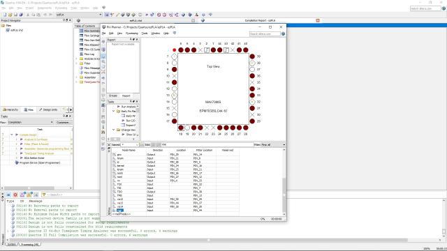
After it's done we need to compile the design again.
We can see here that the whole design has taken 12 of 32 macrocells. So we still have some room left on our CPLD chip.
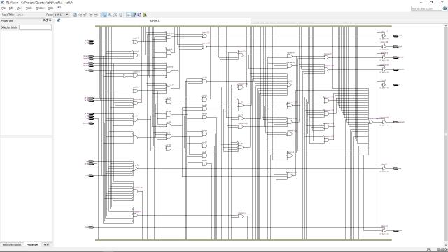
For fun, you can also visualize how the design is implemented using logic gates. Tools -> Netlist viewers -> RTL viewer. You could even use this design and try to make the PLA chip out of 7400 series chips.
At this point, we are finished with the code. In order to program the chip, we can use the USB-Blaster. But first, we will need to install the drivers for it. After inserting the device into the USB port Windows will recognize it, but won't install the drivers. We can do that inside the Device Manager by right-clicking on the USB-Blaster icon and selecting to update the driver. Then we can browse for its location inside the installed Quartus drivers folder and after a while, the drivers should be installed on your system.
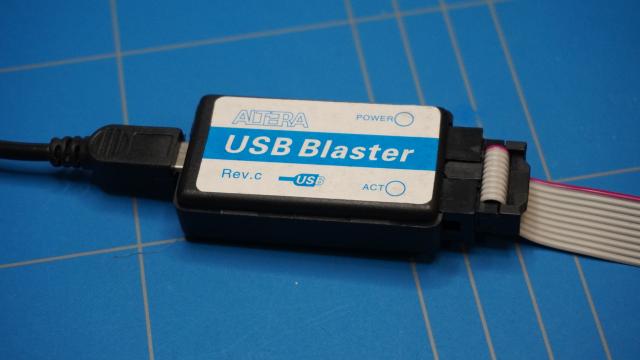
The next step would be to program the chip. Unfortunately, we are not using a development board and can not simply plug in the USB cable and be done with it. We will need to make the connections of all the JTAG pins ourselves.
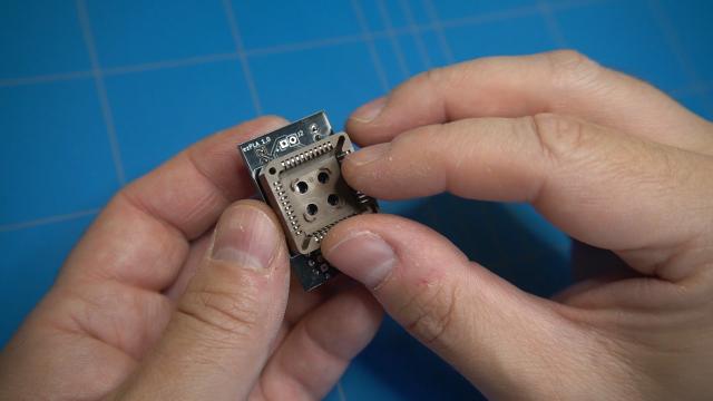
As I mentioned before I have made this prototype board and soldered some pin header onto it. It worked fine, however, the look of this board was not very appealing so I have designed a PCB. Let's assemble it.
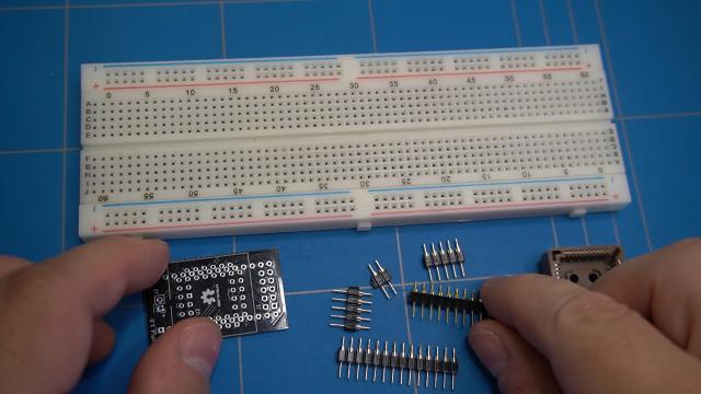
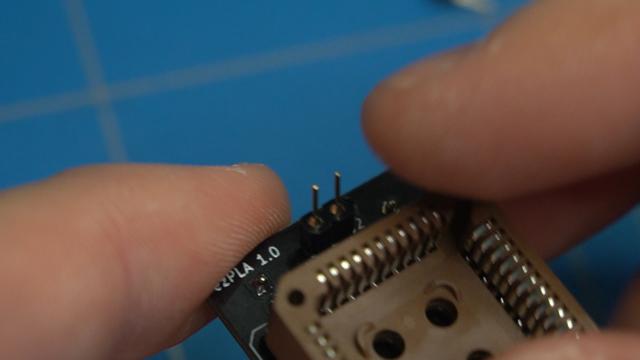
We will start by inserting the thin rounded pin headers on the bottom of the PCB and insert them into the breadboard for easy soldering, then we can solder all the pins and give it a quick rinse with IPA.
Now we will need a PLCC44 socket. Luckily I still have some in stock.
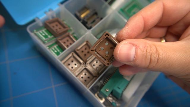
We can insert it on the front of the PCB. Pin number 1 should be located in the top left corner proceed to solder the socket. It is a bit tricky as the pins are close to the headers.
Now we can insert the programming headers and the small 5V pin header. We need to provide 5V to it from another source as the USB-Blaster programming header will not do that. I have also glued some blue tack on the pins so they won't move while soldering.
We can now insert the Altera chip into the socket and insert the USB blaster pin headers and provide the chip with 5V of power.
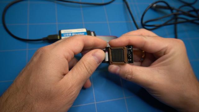
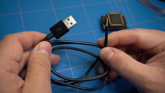
Oh.. btw.. I have made the 5V power supply out of an old USB power cable by attaching a 2-pin header onto it. Anyhow... we are now ready to program the chip.
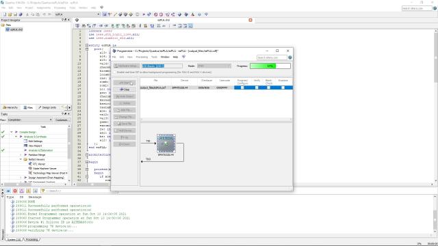
When we click on the programmer icon inside Quartus and then on the Hardware Setup button we can choose the USB-Blaster as the currently selected hardware. Then we can specify the file that we want to program onto the chip. This file was previously compiled and stored inside the output files folder. Now we can select the program and verify checkboxes and click on the start button to program the chip. After a short while, the CPLD chip will be programmed.
Let's insert the freshly programmed chip into the Commodore 64 PLA socket to see if it works. And it does! At least in the 250425 board revision. I will still need to make more tests to see if it works in Commodore 64 computers with another board revision.
I have made all of the KiCad design files and the Quartus VHDL code available for free download.
Kicad design files of ezPLA (In this design the CPLD chip is placed inside a PLCC64 socket)
Thank you for reading this blog and I hope to hear from you in the future.