The most important chip in commodore 64 computer is the PLA chip. When this chip is broken, nothing will work and most certainly you will get a black screen after you try to turn it on. The original replacement chip is hard to get and if you find one it is not cheap. Luckily there are alternatives for replacement. It is possible to create one using EPROM, however the results of it's performance vary, or you can buy one on the market like SuperPLA, realPLA, U17 PLAnkton or PLAtinum. Those chips are based on CPLD chips and are programmed with logic that perform the same function as the original PLA chip. In our project we are going to create a PLA chip using Altera EPM7032 CPLD chip.
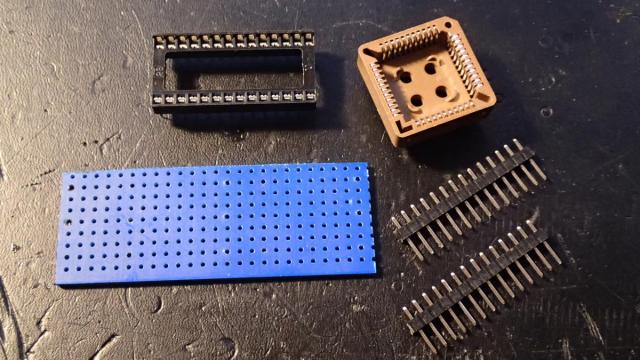
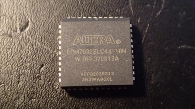
First we are going to build a JTAG programmable Altera CPLD board which will have DIP 28 pin chip output. For that purpose we will need a couple of parts. These are a universal PCB board which has 25 x 9 holes. I have cut mine from a larger piece that I had lying around. Then you will need a PLCC44 socket, DIP28 socket, some DIP pin header connectors and of course the Altera chip. It doesn't need much capacity for storage. 32 macrocells is large enough. I have chosen Altera EPM7032SLC44-10N. They are very cheap and you can find them for around 1 euro a piece.
The other advantage of this chip is that it is powered by 5V and has 5V tolerant I/O ports. So it can be directly powered from the PLA chip socket on the C64 motherboard.
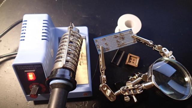
What the combination of this part will give you is DIP compatibility, which translates to relatively easy soldering. So let's start building our FPGA / CPLD programmers board with JTAG programming capability.
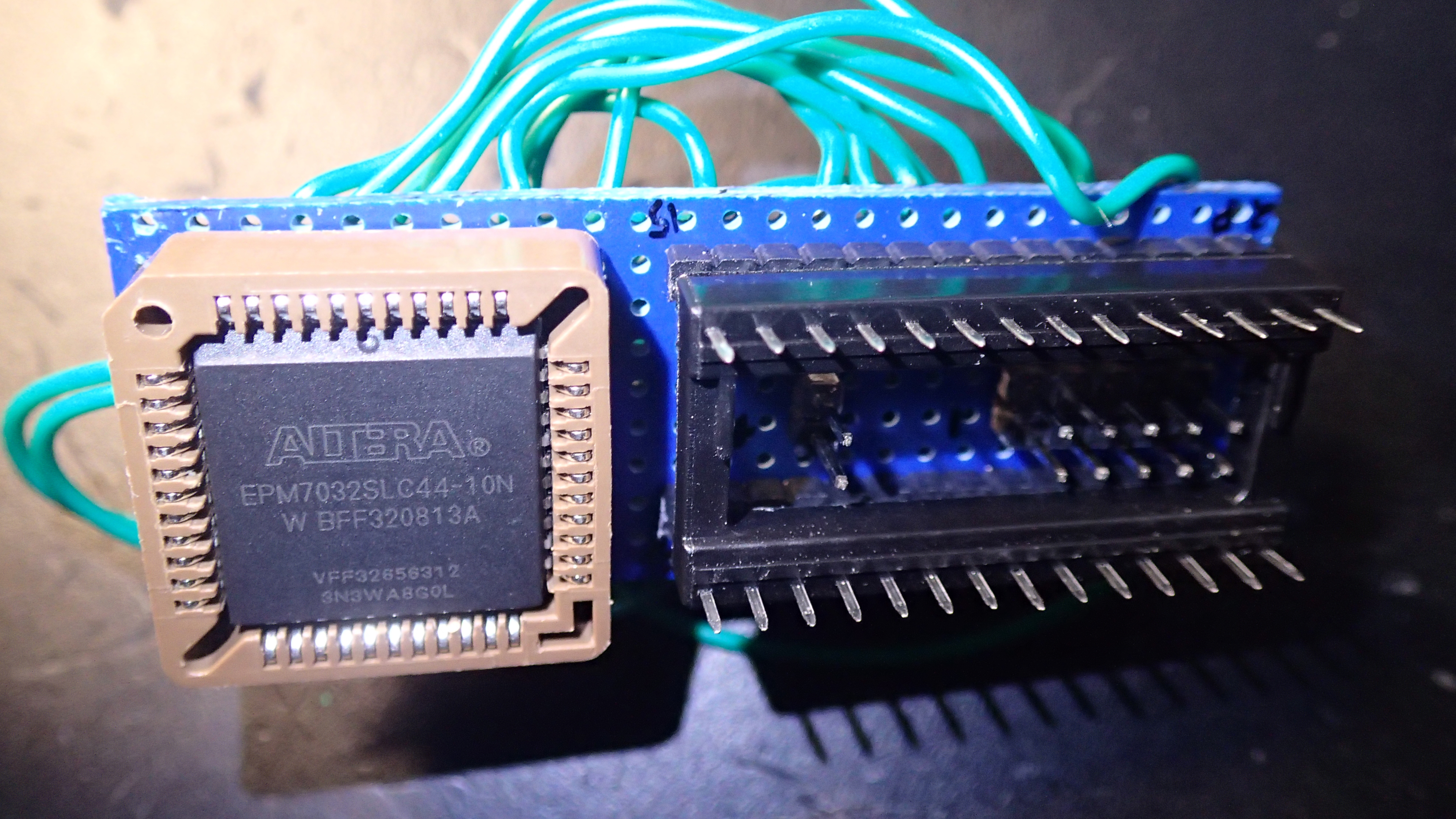
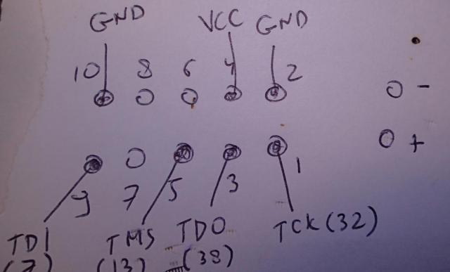
The Altera CPLD chip has 4 reserved I/O pins which can be used to program the chip. These pins are TCK (pin 32), TDI (pin 7), TDO (pin 38) and TMS (pin 13). The JTAG interface will also need 5V and GND connections. The power needs to be supplied to the JTAG port and not the other way around (as I have found out after some time of troubleshooting the JTAG port). These are the 2 pin headers next to the 10 pin JTAG header. The "1" written next to the pin with the black marker is where the TCK signal will be connected.
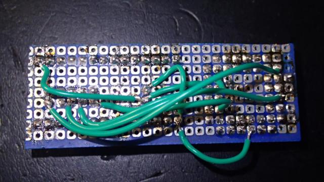
Now we need to connect the PLCC44 socket pins to our JTAG port and the power pins. I have found this nice schematic online (which is from www.digital-circuitry.com).
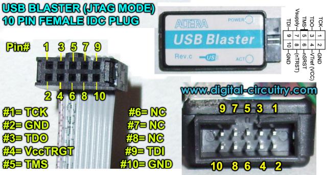
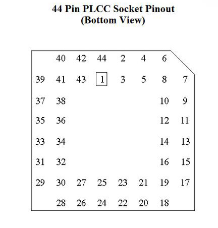
This is the bottom view of our JTAG pinout.
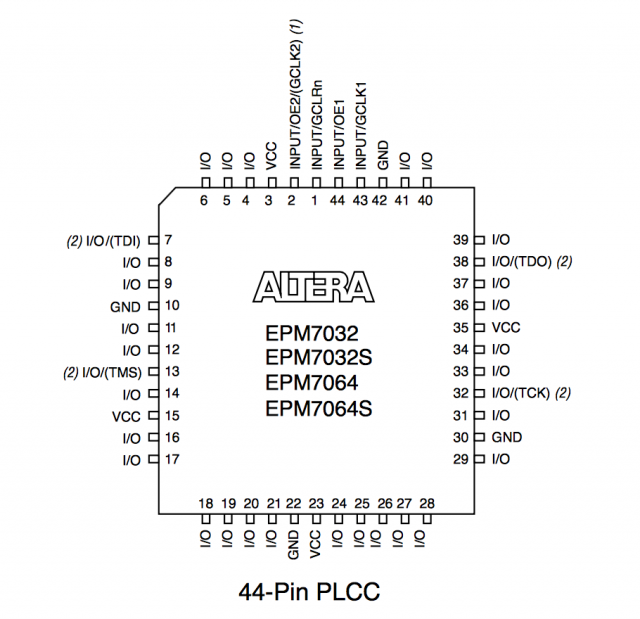
These are the pinouts of the Altera 7032 chip:
And the bottom view of the PLCC44 socket:
This is what you will need to solder:
| JTAG pins (on our board) | PLCC44 socket |
| 1 (TCK) | 32 |
| 3 (TDO) | 38 |
| 5 (TMS) | 13 |
| 9 (TDI) | 7 |
| 4 (VccTRGT) | 15 (VCC) |
| 10 (GND) | 10 (GND) |
Also connect the VCC (5V pin socket) and GND to the separate 2 pin header. You will need to supply 5V power to this header pin in order to program the chip.
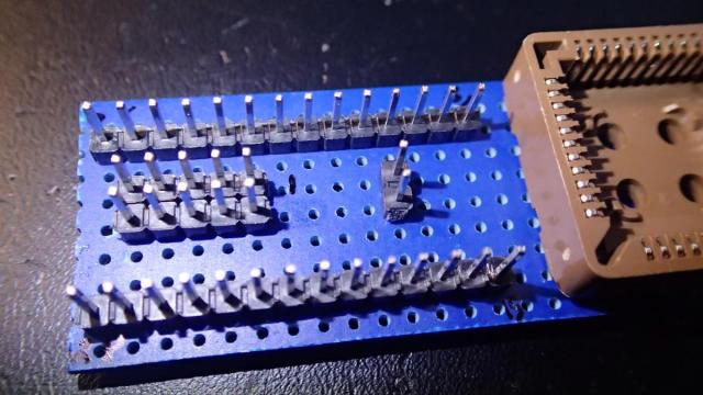
After you are done it will look something like this. Note that this picture misses the connection from the 2 pin (VCC/GND) header to the JTAG port. I took this picture before soldering the extra connection. Programming the chip without them will fail to program the chip!
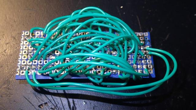
Now we need to connect the remaining I/O pins from the Altera chip to the DIP28 PLA chip configuration. This table provides the remaining connections:
| DIP28 (PLA chip) | PLCC44 socket |
| 1 | 8 |
| 2 | 9 |
| 3 | 11 |
| 4 | 17 |
| 5 | 18 |
| 6 | 20 |
| 7 | 21 |
| 8 | 25 |
| 9 | 24 |
| 10 | 26 |
| 11 | 27 |
| 12 | 28 |
| 13 | 29 |
| 14 | 22 (GND) |
| 15 | 31 |
| 16 | 34 |
| 17 | 33 |
| 18 | 36 |
| 19 | 37 |
| 20 | 39 |
| 21 | 44 |
| 22 | 6 |
| 23 | 5 |
| 24 | 4 |
| 25 | 1 |
| 26 | 41 |
| 27 | 40 |
| 28 | 35 (VCC) |
After you are done it will look something like this. Don't forget that we are prototyping. Next step would be to create a PCB in a software PCB layout tool like KiCad.
We are now ready to create a project in Quartus II and define how the PLA chip behaves.
In 2012 Thomas Giesel has dissected the workings of the C64 PLA chip. And in 1986 in Volume 6, Issue 05, pp. 51 of The Transactor magazine William Levak from Ann Arbor, Michigan has described the inner workings of the chip and effects on the access of various parts of the Commodore 64 architecture.
If you are up to the challenge you can create logic tables from the information provided above, but there are already other smart people that have done this and created VHDL code out of the information provided above. So I chose to use their skills and use it in this project.
Frank Bass is one of these people. On github I have found his project where he wrote VHDL code that will mimic the behaviour of the PLA chip.
I just needed to create a block diagram and connect the correct pinout.
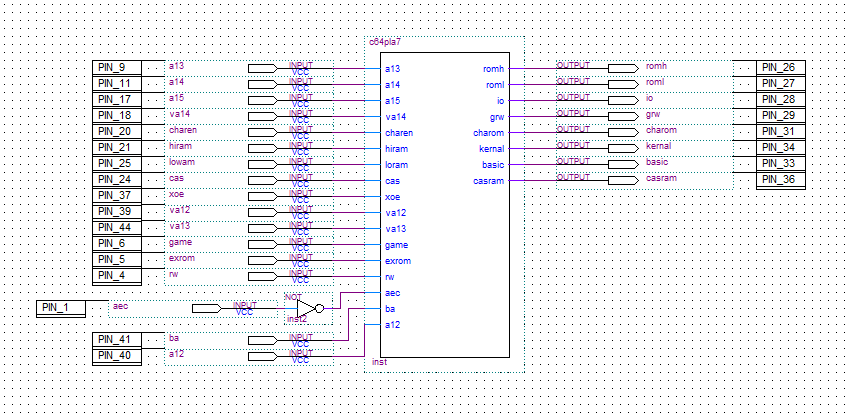
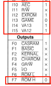
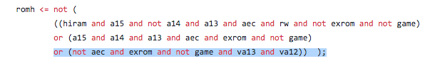
Because of the logic in the VHDL code note that pin 1 (AEC) needs to be inverted. As you can see on page 52 inside the Transactor issue the combination of inputs AEC (1), EXROM(1), GAME (0), VA13 (1) and VA12 (1) are causing the ROM H output to be set LOW.
And inside the VHDL code you can see that the aec variable is being inverted. It is possible to fix it inside the code, but I was just being lazy and added the NOT gate inside the block diagram. :-)
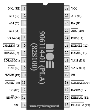
To make this information complete I have also attached the original pinout of the PLA chip.
You can download here the Quartus II project that I have created.
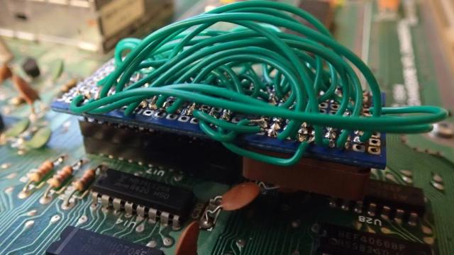
And this is how it looks on the C64 motherboard.
I hope that you can learn something from the information that I have gathered and provided in this blog. If you have any questions, you can always contact me.