A while back I created a prototype board for the PLA replacement chip for C64. It was time to make a PCB out of it. In this blog post I will describe the steps that I did to design the PCB using KiCad and manufacture it using PCBWay prototype service.
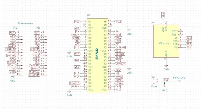
Let's start to create the schematic in KiCad based on the connections that are made in the PLA prototype board. This schematic is using 2 custom symbols for the PLA-headers and the CPLD chip. To make the schematic a little bit more clear I have made the connections using global labels. The symbols on the right are for the JTAG header and for the power supply.
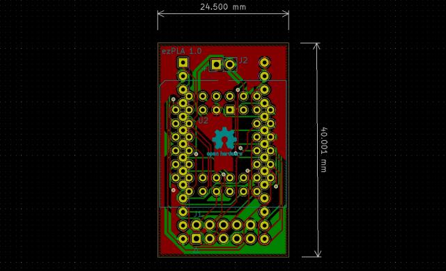
Then I created 2 custom footprints. The first is for the PLA-headers, which is based on a DIP-28 15.24mm wide socket, only reversed. And the second one is a 2x5 IDC header with some small adjustments in the silk screen. After that it was just a matter of assigning the correct footprints to the symbols. To make all the traces I have used open source Freerouting software.
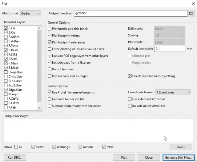
It was time to generate Gerber files and upload them to the PCBWay website. The gerber files need to include the following layers. The rest of the settings can stay as default.
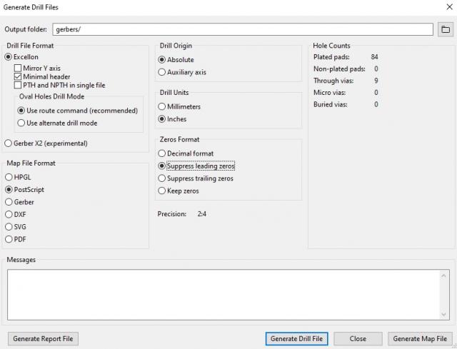
Next you will need to generate Drill Files. Make sure you have selected "minimal header" and "suppress leading zero" options. You can also check the "PTH and NPTH in single file" checkbox, but PCBWay can handle both options.
You can zip all files and upload them on the PCBWay website. I have also created a shared project on PCBWay that already includes the correct files for the ezPLA PCB, so you can also order them with a single click. You can also check my GitHub reporisoty that contains the KiCad files.
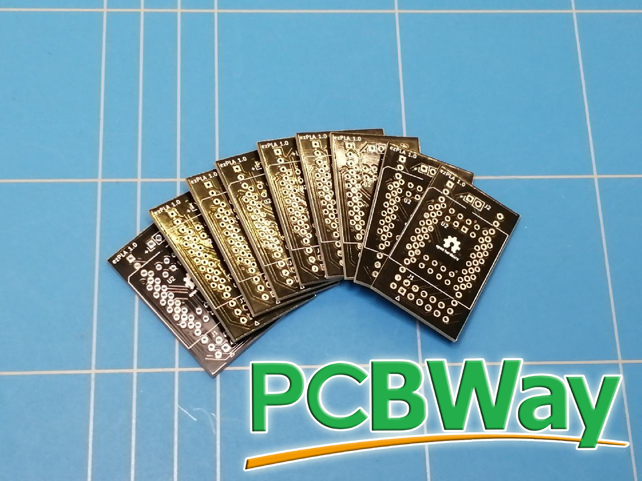
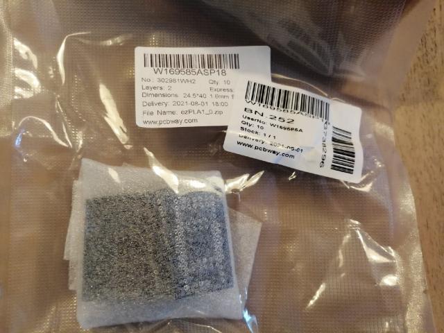
It took two weeks for the order to arrive, but I have selected one of the cheapest options for shipment. Unfortunately the Dutch customs also held it for a week before it got delivered. The PCBs were neatly packed.
In the next blog post I will describe how to solder the PCB and program the Altera EPM7032 chip.