There is something about blinking leds. Numerous projects are created with the 555 timer chip. To continue the tradition I will describe in detail the creation of a 555 astable timer board that was designed in the previous blog post.
The PDF export for the previous post was just a single inverted negative. The PDF page dimensions were equal to the board. In order to create a good UV mask, we will need 2 layers on top of each other and some layer alignment targets. We also don't want to be wasteful on the transparent overhead projector (OHP) sheets so we will print it in an area where we can cut it off and reuse the remaining of the sheet.
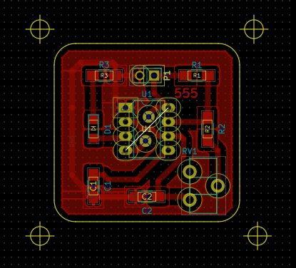
First lets add alignment targets to the layers in KiCad. Use the Add layer alignment targets ![]() icon and place them in the corners of the PCB design.
icon and place them in the corners of the PCB design.

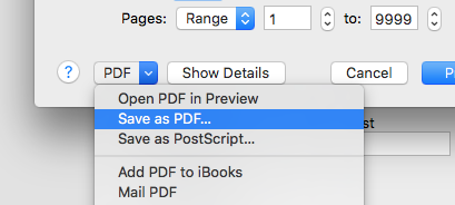
Now print the design to PDF format by selecting Print from the File menu, pressing the Print button and choosing save as PDF option.

Load the PDF into Illustrator and follow the steps from previous post to invert and mirror the design. Now we are going to duplicate the design by selecting it all (cmd + A on Mac) and copy / pasting it.

In order to change the printing area to A4 select Document Setup... from File menu and click the button to Edit Artboards (you can also use Shitf + O keyboard shortcut). Now the active artboard will be highlighted. Press Enter and Artboard Option will show up. In the Preset select A4 and change the orientation to Portret mode, then click on OK.

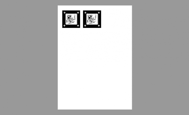
Zoom out so you will see the whole page and select all (cmd + A on Mac). Drag the two designs to the top of the page. The only thing remaining in this step is to save it as PDF.

Now open it up in Adobe Reader and print to an overhead sheet. Make sure you don't change any proportions and always print actual size.
After printing it on the overhead sheets and overlaying the two layers using the layer alignment targets we have a negative that we can use for the exposure.
I have decided to use the iron this time to apply the dry film to the copper layer of the PCB. First I made sure that the temperature of the iron is at around 85 °C.
Then I have placed the PCB with the dry film on top between a folded sheet of paper and pressed hard for around 30 seconds.
The attachment of the dry film turn out better than using my previous technique with the desoldering heat gun.
After the exposure to the UV led light for 5 minutes, the dry film looked like this:
After the bath in Sodium Carbonate for 15 minutes the result looked promising.
The etching process was remarkably slower than the last time. I am not sure about the reason and will have to investigate it. I am guessing that there was not enough cupric chloride and maybe the temperature was lower than last time that I have done it. But after one hour in the solution I was happy with the result.
I drilled some holes for the DIP components. The macro lens of my camera makes it look like it was much larger, but in fact the size of the board is 3 x 3 cm.
It was time go gather all the needed components. My bill of materials was as following:
- NE555P chip (DIP)
- 1M potentiometer (DIP)
- 2x 1K resistors (1206 SMD)
- 1x 220 ohm resistor (1206 SMD)
- 1x 10nF capacitor (1206 SMD)
- 1x 1uF capacitor (1206 SMD)
- Green LED (1206 SMD)
- 2 pin header
- A piece of wire for the bridging connection
It was the first time that I was going to solder SMD components, but it went smoother than I expected. I have used magnification glasses and needle nose tweezers.
After all the components were soldered the board looked like this. It was time to connect 5V power supply using the pin headers and test it. I was lucky and it worked the first time!
