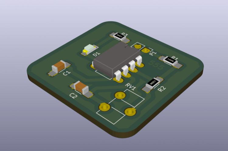
KiCad is a great schematic and PCB design tool. It is easy to learn and fun to use, above all it is free. In this blog post we are going to design a simple circuit based on the 555-timer chip in astable mode.
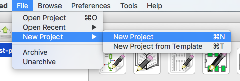
Create a new project in KiCad (File -> New Project -> New project). Best practice is to create a new directory per project. Type in the file name and click save. Initially there are 2 files generated *.kicad_pcb (for the PCB layout) and *.sch (for the schematic).
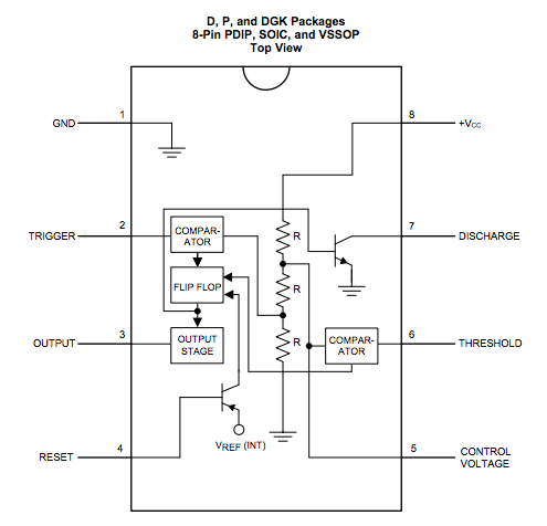
First we are going to create the 555 chip component. (This component is already present in the default KiCad library, but for sake of learning we will create it anyway). First lookup the datasheet for LM555 chip and look for the page with pinout.
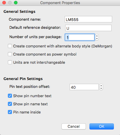
Go to Tools -> Run Library Editor (or press cmd + L shortcut), click on ![]() icon to create the new component and specify the component name.
icon to create the new component and specify the component name.
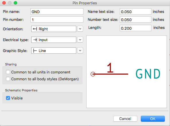
Fill in the pin name with corresponding pin number. Do this for all the 8 pins.
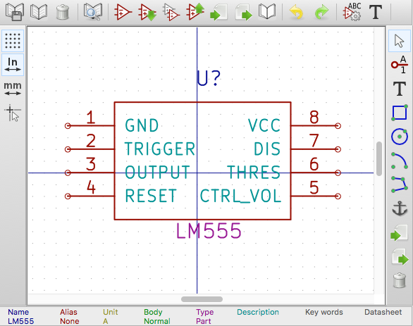
Place the pins in a patters that resembles the one on the datasheet and draw a rectangle around it using this ![]() icon. Move the texts out of the way using the M keyboard shortcut.
icon. Move the texts out of the way using the M keyboard shortcut.
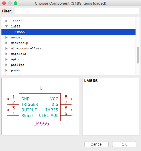
Now save current component to new library by clicking this ![]() icon and save to your project folder. Double click the schematic file (*.sch) in the project view and load up your freshly created library. This is done in the Preferences -> Component Libraries menu item. In the dialog window click on the Add button and browse for the library file (*.lib). When you click on the Place Component
icon and save to your project folder. Double click the schematic file (*.sch) in the project view and load up your freshly created library. This is done in the Preferences -> Component Libraries menu item. In the dialog window click on the Add button and browse for the library file (*.lib). When you click on the Place Component ![]() icon in the schematic window you will see your library with the new component inside it.
icon in the schematic window you will see your library with the new component inside it.
Place this component inside the schematic window. In the same way you can add other parts. In the filter input field, type the names and add them. We are going to need GND, +5V power (press P key as shortcut), Resitors (type R in the filter), Capacitors (type C in the filter), Potentionmeter (POT keyword), LED and a 2 pin header connector CONN_01X02. Arrange the components like in the schematic below.
Below are some handy shortcuts that you can use:
- R - Rotate component
- M - Move component (without the wires)
- G - Move component (with the attached wires)
For the schematic not to be "messy" you can use labels. Use global lables icon ![]() to place them.
to place them.

After you are done click the annotate icon ![]() in the toolbar. This will annotate all your components in the schematic, so R? wlll become R1, R2, etc.
in the toolbar. This will annotate all your components in the schematic, so R? wlll become R1, R2, etc.
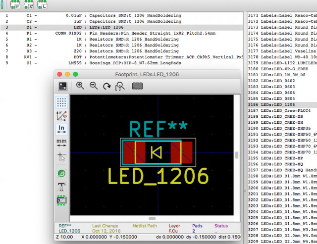
On of the last things left to do is to associate schematic symbols to PCB footprints. Click the CvPcb ![]() icon and a large window will pop-up with all the components that you have added to your schematics. First press the preview
icon and a large window will pop-up with all the components that you have added to your schematics. First press the preview ![]() icon in the toolbar. Now when you select a component you can assign it to a footprint inside the frame on the right. I am using some 1206 SMD alongside larger DIP components.
icon in the toolbar. Now when you select a component you can assign it to a footprint inside the frame on the right. I am using some 1206 SMD alongside larger DIP components.
As last generate the NET list file, which will be used in the PCB layout. Simply click on the ![]() icon and choose the default Pcbnew format. Save the netlist (*.net) in your project directory. We are now done with the schematic and are going to move to the PCB layout view. Close the schmatic window and double click the (*.kicad_pcb) file or use the Pcbnew icon to open it.
icon and choose the default Pcbnew format. Save the netlist (*.net) in your project directory. We are now done with the schematic and are going to move to the PCB layout view. Close the schmatic window and double click the (*.kicad_pcb) file or use the Pcbnew icon to open it.
In the PCB view load the generated NET list file. You will get a bundle of components on top of each other.
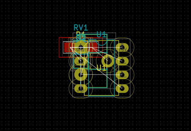
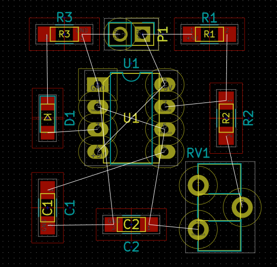
Use the M (Move) and R (Rotate) key shortcuts to separate them in the layout. All the components are connected with so called rubber bands to show the existing connections. Try to minimize the intersecting of the wires and make a nice layout.
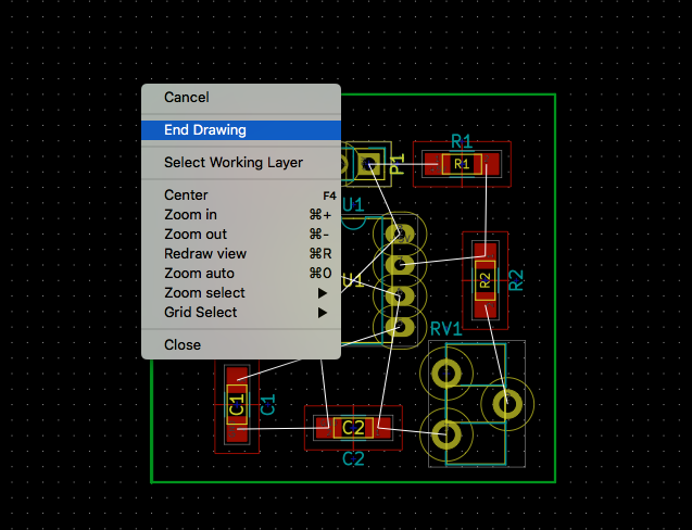
Let's create a board outline with rounded edges. First we need to create a rectangle that will help us. Select the Eco1.User layer in layer tab. ![]() . Notice the blue arraw that is pointing towards it. Using the line tool
. Notice the blue arraw that is pointing towards it. Using the line tool ![]() start drawing edge lines. Right click when you end drawing the last line and select End Drawing from the pop-up menu.
start drawing edge lines. Right click when you end drawing the last line and select End Drawing from the pop-up menu.
Now choose the Edge.Cuts layer ![]() and select the arc tool
and select the arc tool ![]() . Draw arcs on the edges on the green rectangle.
. Draw arcs on the edges on the green rectangle.
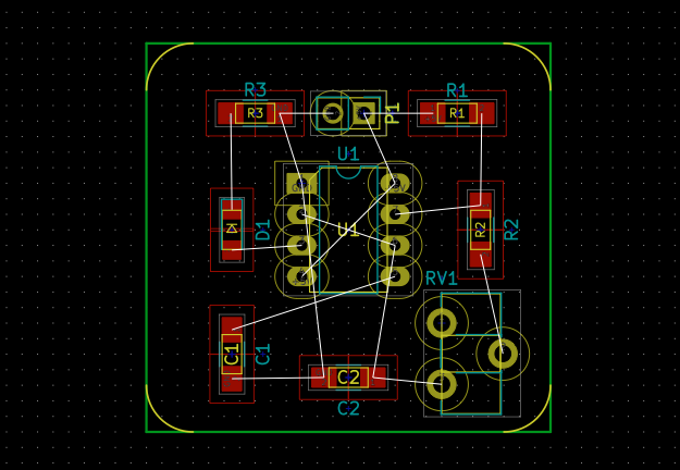
Using the line tool connect the yellow arcs and delete the green Eco1.User layer. Locate the mouse cursor over the green line and press delete button (or fn + backspace keys on Mac). A selection menu will appear. Choose the Eco1.User line and it will be removed.

You should end up with a rounded corners rectangle on the Edge.Cuts layer.
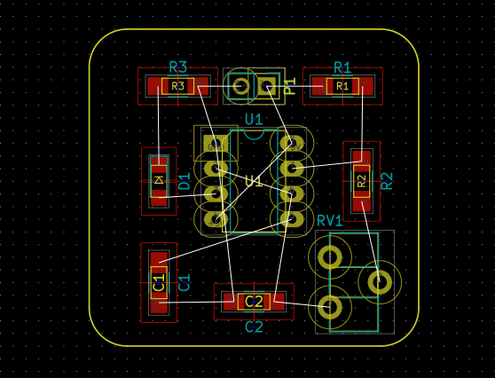
Now we need to route the board and convert the connections to solid tracks. I have chosen to create a single sided board layout as it is the most common in home made PCB fabrication. First switch the canvas to OpenGL mode by selecting it in the View menu. This will enable the interactive router functionality.

Select Add tracks and vias ![]() icon and start replacing the rubber band connection with real copper tracks. Do this on the top copper layer (F.Cu). It works very intuitively. Just click on the points you want to connect and the track will be created. You can also watch the youtube tutorial with detailed explanation.
icon and start replacing the rubber band connection with real copper tracks. Do this on the top copper layer (F.Cu). It works very intuitively. Just click on the points you want to connect and the track will be created. You can also watch the youtube tutorial with detailed explanation.
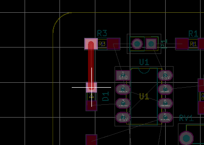
When you are done you should get a result like the one below. Notice in the middle of the board, that there is one connection left open for a bridging wire connection. It's located between the U1 text and it's connection pin 4 to pin 8 of the LM555 chip. Maybe you can create a layout that won't have any bridging connections that are left open, but I spent some time on it and could not do it.

To finish up the routing we can add a filled zone that will cover all the ground connections on the copper layer. Select the add filled zones ![]() icon and click the left mouse button to start drawing. A dialog window will pop-up that will let you specify that you want the front copper layer (F.Cu) and the GND net as the zone properties.
icon and click the left mouse button to start drawing. A dialog window will pop-up that will let you specify that you want the front copper layer (F.Cu) and the GND net as the zone properties.
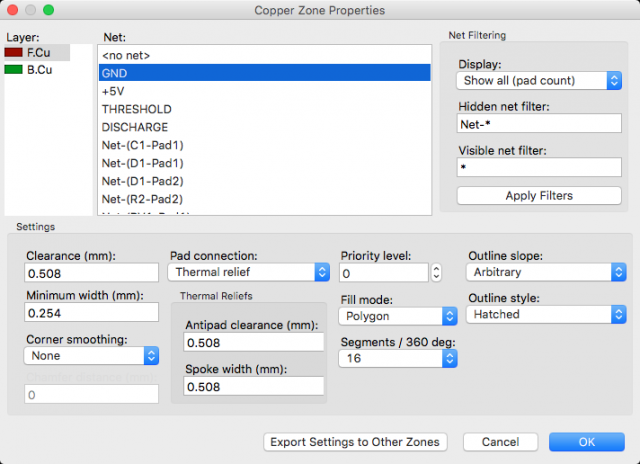
Click on OK and continue drawing the zone. Again, close the zone outline with right mouse click and select the proper item from the pop-up menu.

You also need to fill the zone. To do this right click somewhere inside the area. Select Fill or Refill All Zones. You can also use the shortcut key B.

The finished zone outline should look something like in the screenshot below.

You can switch the visibility of the filled zone areas with the icons illustrated below in the left on the screen.

Notice that there is no zone fill in the upper right area of the board. This is because there is no GND connection on it. It is a nice place to add some logo or text. If you would like to add a logo, you can do this with the add footprints ![]() icon. By clicking on the List All button and the searching for OSHW you will get a nice logo. In my case the area was too small and I decided to add 555 text with the text tool
icon. By clicking on the List All button and the searching for OSHW you will get a nice logo. In my case the area was too small and I decided to add 555 text with the text tool ![]() icon. It fitted perfectly.
icon. It fitted perfectly.
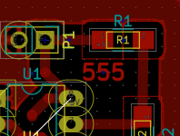
To make the bridging connection a bit better we will add solder wire pads. This can be done by clicking on the add footpints  icon and typing in the filter: SolderWirePad, then selecting SolderWirePad_single_0-8mmDrill. To position the wire pad more precisely hold cmd + shift keys while moving it around. There will be also a REF** text added, you need to edit it in order to get rid of it. Hover your mouse on top of the text and press the E key. A pop-up will appear where you can choose Reference REF***. In the Display group, select Invisible radio button and press OK.
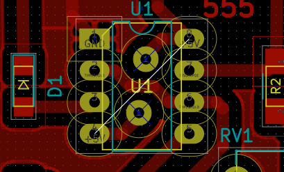
A very cool feature of KiCad is the 3D Viewer function. You can render the board and check how it will look after it's finished. Go to View -> 3D Viewer to access this feature. A preview of this board is captured as the header image for this post.
We are done with the board. What's left is exporting the design into some usable format for the next process. If you want to send the board out for manufacturing you can export Gerber files. To do this select File -> Plot in the menu and specify the layers you want to export. But I was going to etch the board myself and needed different output. First I tried to export the file as SVG and it worked fine, but when I loaded it up in Illustrator the drawing looked corrupt. So then I did File -> Print and saved the design as PDF. Just selecting the F.Cu copper layer. Now it opened without any problem in Illustrator.
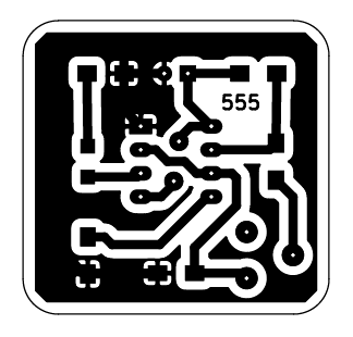
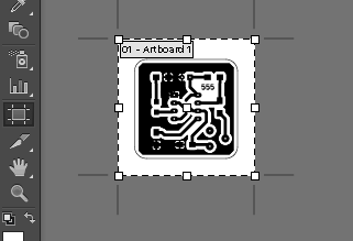
Because I was planning to use dry film and UV exposure technique just as I described in my previous post I needed to invert and mirror the design. This can be done in Illustrator. Start by resizing the board with the Artboard tool to smaller workable area.
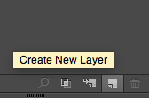
Before inverting we will add a new layer to the design.
Then draw a rectangle with the rectangle tool on the newly created layer.
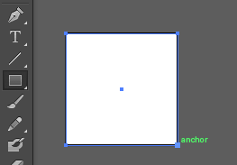
Place the new layer (2) below the PCB design layer (1), then select the whole design (with cmd + A on a Mac) and choose inverting colors from menu: Edit -> Edit colors -> Invert colors.

To finish we will mirror the design in the vertical direction. Go to Object -> Transform -> Reflect ... and select the vertical axis.
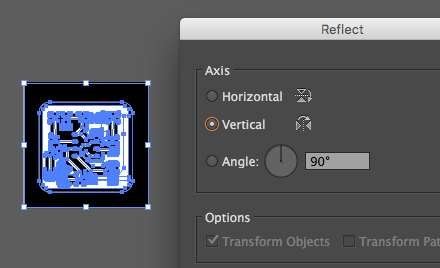
The design is now finished. I you wish you can download this design in PDF format. I have also compressed all the project files.

