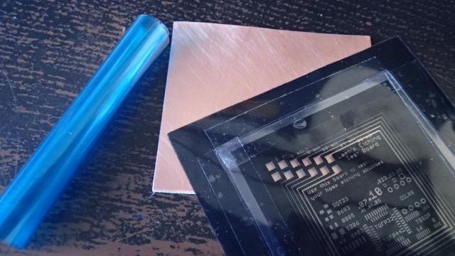
Being able to make your own printed circuits boards is a skill that can come in handy. There are several ways to do this and I will describe the one that I use. First part of the process is the creation of a layer on top of the copper that prevents the solvent to dissolve it.
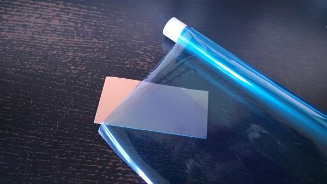
For that purpose we will use Dry Film Photoresist. It is a substance that reacts to UV light and then becomes resistant to the developing solution (which is Sodium Carbonate). You can buy it cheap on Chinese reseller websites.
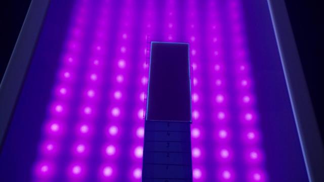
But let's start from the beginning... In the previous blog I have made an UV LED light exposure box from an old scanner unit. We will make use of it in this tutorial. It is not absolutely necessary as you can also use direct sun light, but it's faster to use UV light source.
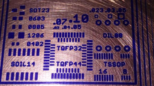
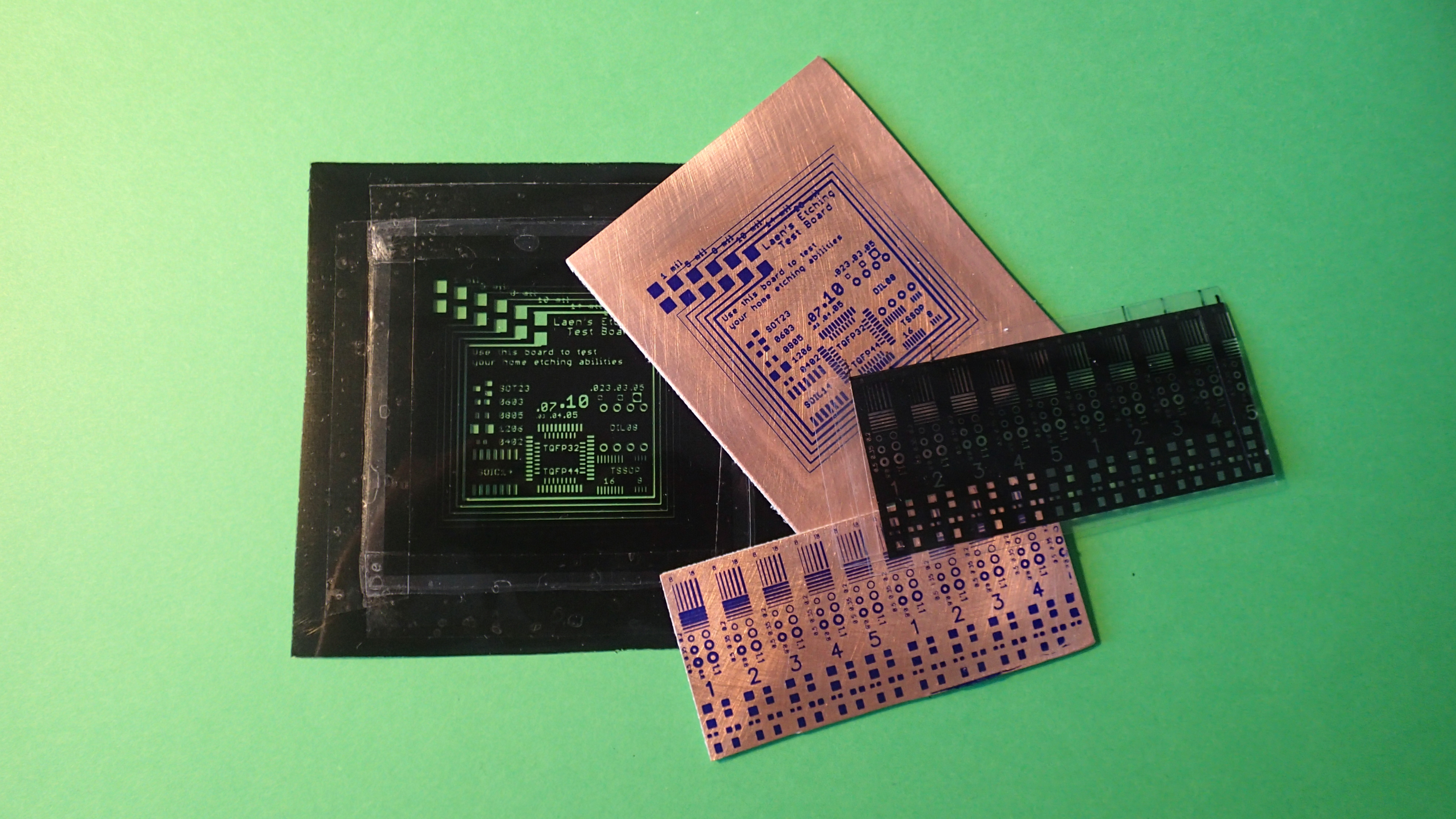
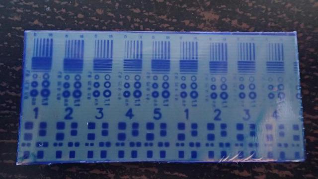
As I stated before we will be exposing the parts that we want to keep, so we will need a negative of the PCB design. Online I have found a couple of designs that can be used for test purposes. They were not completely suitable, so I have changed the original PDFs a bit with Adobe Illustrator. You can download them here. I contains two designs. Print them on a OHP (Overhead projector) Transparancy Film.
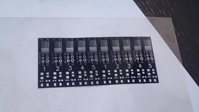
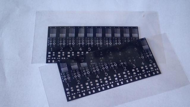
The first one is to test the UV light exposure time.
And the second one is more for allround testing and etching purposes. The designs in the PDF files are mirrored. This way the printed layer will be in direct contact with the copper layer, preventing the light to pass at an angle.
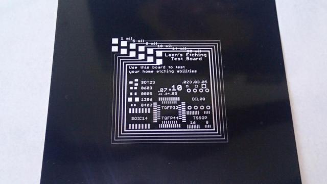
I have also printed them twice and placed the sheets on top of each other as I have noticed that they were not dark enough and light was still passing through it.
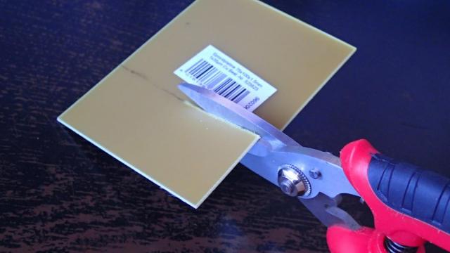
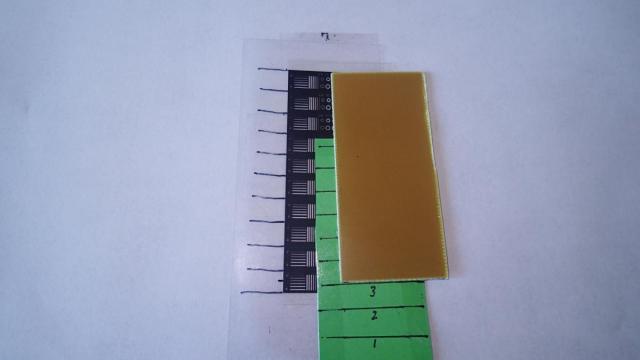
It was time to prepare the board and cut it to the right size. I have used sheet metal cutter scissors. This cut would split the board into 2 pieces that were good enough to apply the testing designs.
Next, scrub the rough edges with a file.

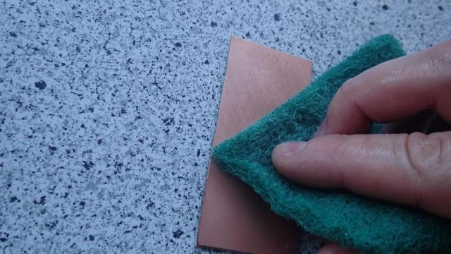
Before applying the dry film, you need to clean the board with acetone and scrub the surface with (optimally) steel wool. But I have noticed that a scrubber sponge works as well...
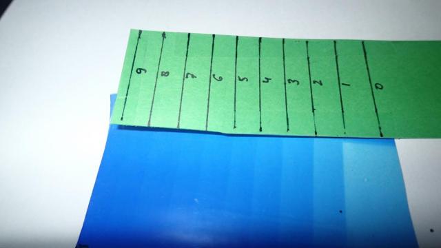
To test the exposure I have created a slit of carton paper with numbers, that could be layered between the mask and the board and slided down at given time intervals.
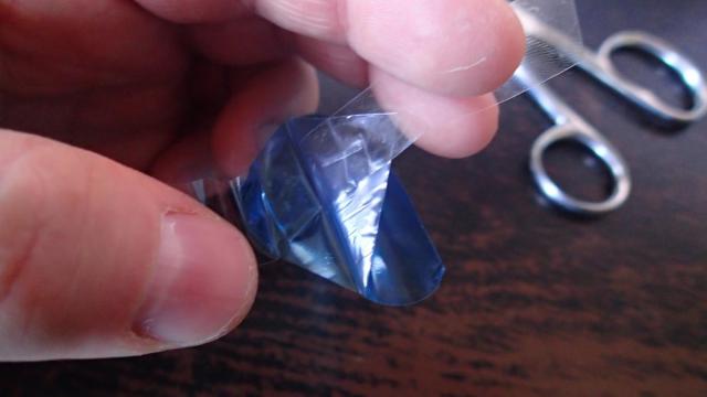
The dry film is protected with two layers. To apply it to the PCB you must remove the inside layer. Stick scotch tape on both sides and gently separate them.
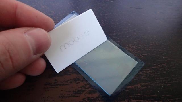
Then apply it and use a credit card to squeeze all the bubbles out.
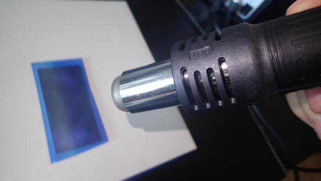
Now you need to heat up the film so it will attach to the copper layer. There are several methods to do it. In my case I have tried the laminator and the iron, but they were too hot and the substance melted and spreaded out unevenly. So I used a desoldering heat gun set at a temperature of 200 degrees celcius and blew it on top of the board for around 2 minutes. I noticed that you need to give some extra attention to the corners.
Now let's test the exposure. I have placed the board with the sliding carton paper on top of the UV light source and exposed in intervals of 30 seconds.
These were the results. The best exposore times were between 3:30 and 4:30 minutes.
This is another test that I did, with just the dry film. You can see the relation in colour and exposure times as the longer exposure darkens the film. Starting from 1:00 to 5:00 minutes.
I have repeated the process for the other design.
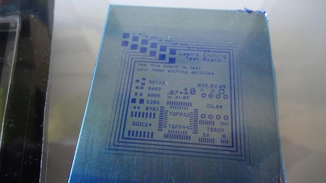
I exposed this board for 4:00 minutes.
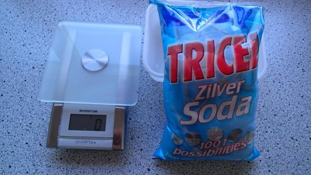
It was time to develop the board. For this purpure I have used sodium carbonate, which also goes by the name of cleaning soda and you can buy it dirt cheat at the supermarket. I payed 69 euro cents for 1 kilo.
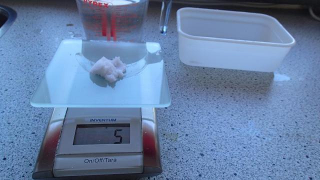
Measure 5 grams (which is about a teaspoon) and solve it in 500 ml of water.
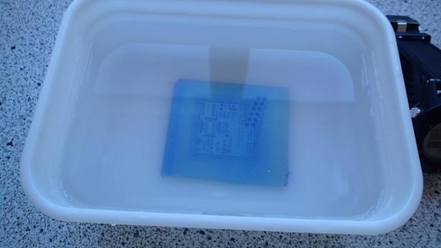
Remove the top protective layer of the dry film and place it in the solution for 4 to 5 minutes. Use a soft brush on the board from time to time to remove the dissolving substance.
This is the final result after a finished developing process.
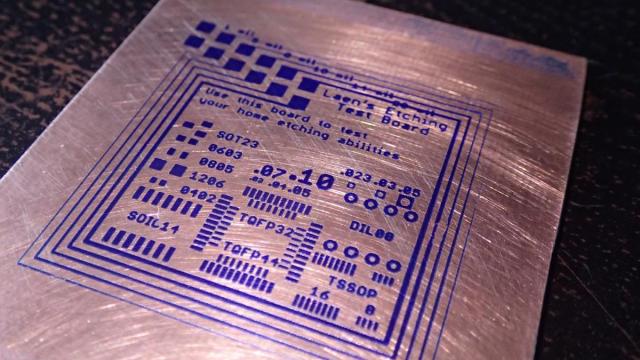
And a close up