The most important part of a computer architecture is a clock circuit. The circuit described here has the option to run freely in a-stable mode and also operate in single step debugging mode. In this post I will describe how to implement this design in KiCad and manufacture a double sided printed circuit board.
A good way to learn how a computer operates is to analyse and build a SAP (simple as possible) computer architecture. It is described in a book by Albert P. Malvino with the title Digital Computer Electronics and it shows all the parts that are present in a computer design. Before we can start with the architecture we will need to build this clock circuit. It is initially designed and presented in a youtube video tutorial by Ben Eater. Although I have build this circuit on a breadboard I wanted a stand alone small PCB module with SMD components. This will be a start in order to complete my SMD based SAP1 computer.
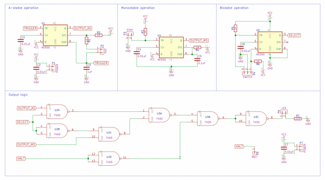
The schematic of this circuit is based on three 555 timer chips and two NAND logic gates. What is nice about this design that it illustrates 3 scenarios on how to implement the 555 timer. First sub-circuit is an a-stable mode which just pulses the output with a variable frequency that is adjustable with the potentiometer. The next one is monostable operation where the chip is used to debounce the button. This way it will not trigger multiple pulses when you push the button in stepping mode. The last is the bistable operation which just uses the RS latch inside the timer chip to debounce the selector switch. It ties to the logic function, that makes it possible to make a selection between the a-stable and monostable operation of the clock.
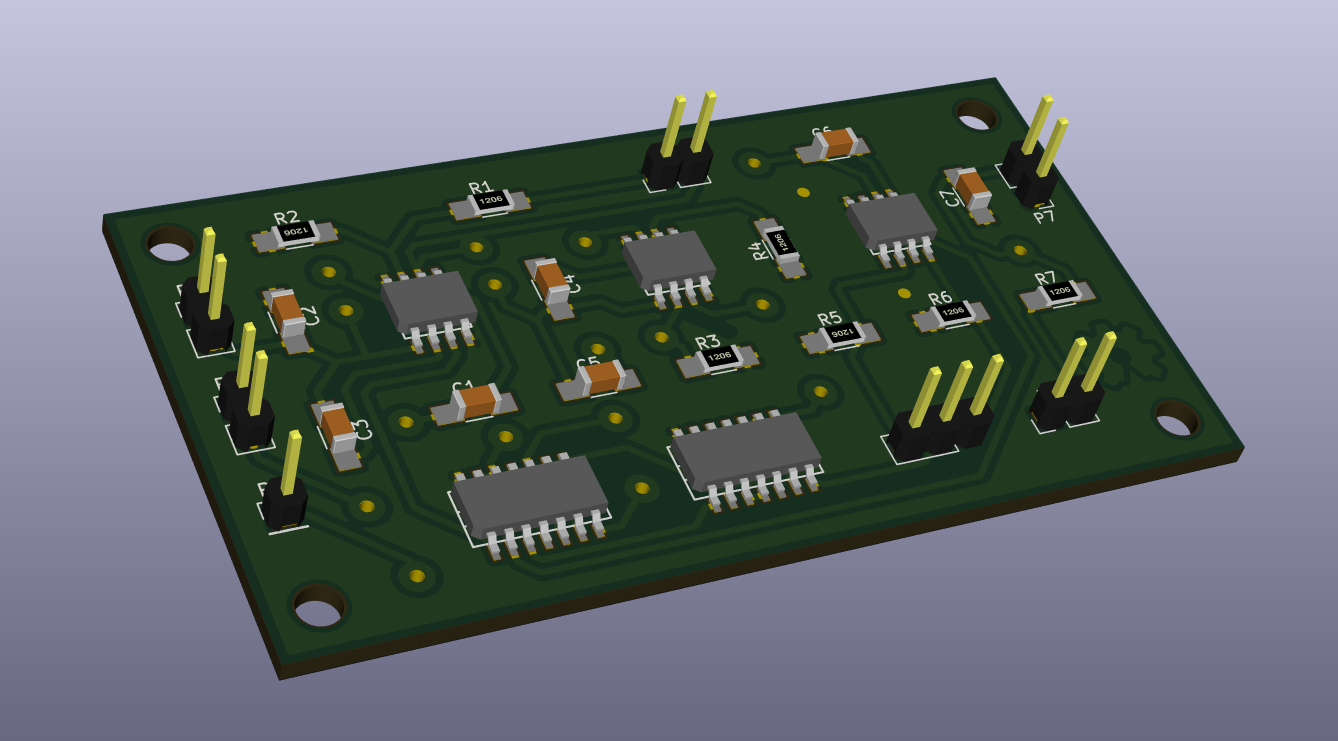
The idea of the PCB design was so it can be placed in a box and controlled by externally installed switches. I have also added second power connector so you can chain power to other modules.
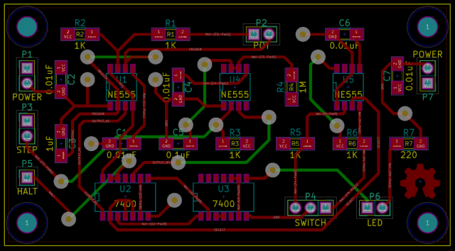
At first I tried to design the PCB so it would be single sided, but I couldn't route it without connection on the back of the board. Then I have decided to design a double sided PCB. I needed to create large VIA pads, because I was going to make them manually and the smallest drill that I had was 0.8 mm in size. The VIA pad was 2.5 mm in diameter. Because of my home made manufacturing process the design rule for the track width and clearance was 0.5 mm. The SMD components that I have used were 1206. This way there would not be a problem during the manual soldering process. The package of the 555 timer was SOIC-8 and the 7400 chip was SOIC-14.
Download KiCad files from Github (including the PDF page listed below).
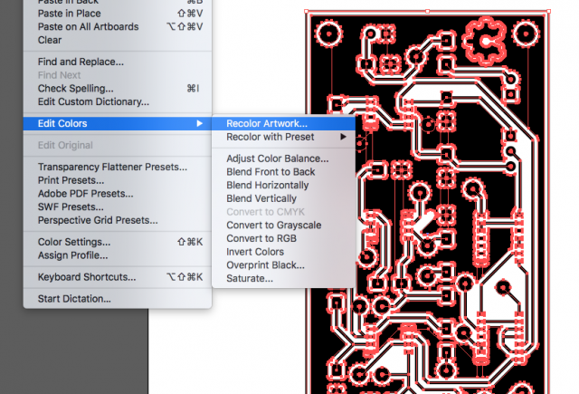
It was time to create the board. After printing the PDF in KiCad, I have noticed that the 3mm drill holes on the sides has a yellow fill-in color, even that I have chosen to print it in black and white. So I had to correct this problem in Illustrator. This is easy as there is a option to recolor the design under Edit -> Edit Colors -> Recolor artwork. First select everything (cmd + A on the Mac) and then run the function.
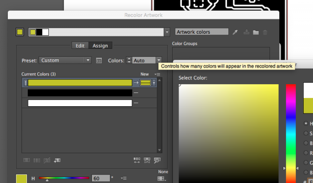
A form will pop-up that will let you change colors. Choose the color you want to replace and select a substitute. In this case it was white.
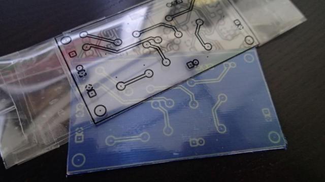
Then I have printed the negatives on an OHP sheet. I needed 2 prints of each. Taking possible errors into account I printed 3 designs for each side. Sometimes it happens that the overlay of the prints do not match, this is caused by deformation of the sheet by the laser printer. Another thing to be taken into account is that the bottom layer does not need mirroring, so the toner layer attached to the sheet will be in direct contact with the dry film layer.
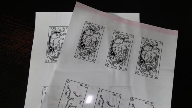
The ticky part was to align the top and bottom layer as I needed to keep the fact in mind that there is a 1.5 mm thick PCB between them.
After 6 minutes of exposure in the UV light it was ready. This is the top layer:
And the bottom layer:
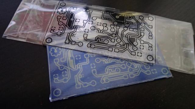
After devloping the PCB in 1% sodium bicarbonate solution (Na2CO3) for 6 minutes, then etching in cupric chloride (CuCl2) for 2 hours and finally taking off the remaining dry film layer with sodium hydroxide (NaOH) the board looked like this:
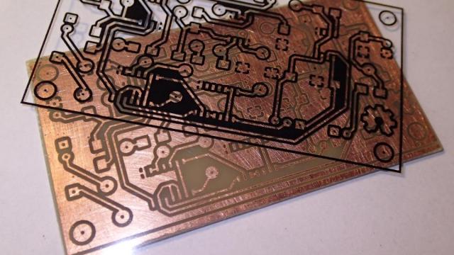
And the bottom layer:
The tracks were all fine, there was only some etchant that run under the edges of the board.
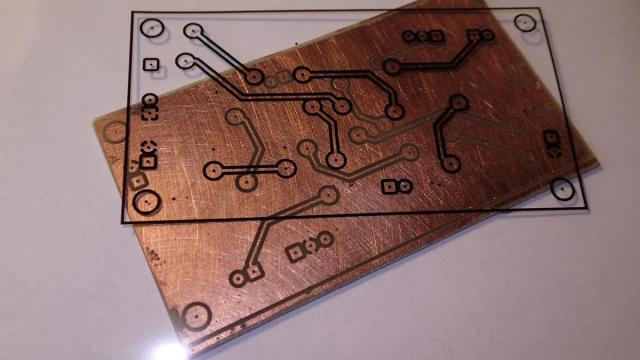
It was time to drill the holes. I have used a Dremel workstation with 0.8 mm drill.

It came out looking fine. The 2.5 mm VIA pads might be even a bit too large. Comparing to the diameter of the pin header pads which were 1.7 mm in diameter and a tiny bit too small. I think that optimal size for both pads would be 2.0 mm. The holes on the size were drilled with a 3.2 mm drill.
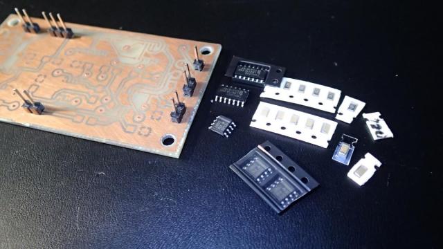
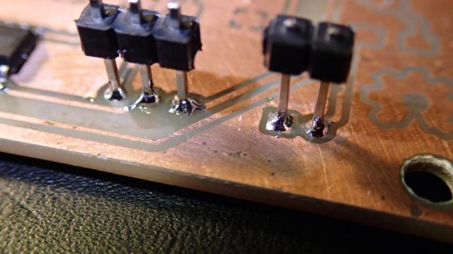
I have collected the needed parts and also attached the pin headers to the board.
The complete BOM:
- 3x NE555 chip (SOIC-8 package)
- 2x 74HC00 NAND chips (SOIC-14 package). They are CMOS, but turn out to work fine with TTL logic on 5V.
- 5x 10nF (0.01uF) capacitors (SMD 1206)
- 1x 100nF (0.1uF) capacitor (SMD 1206)
- 1x 1uF capacitor (SMD 1206)
- 5x 1K resistors (SMD 1206)
- 1x 220 ohm resistor (SMD 1206)
- 1x 1M ohm resistor (SMD 1206)
- A strip of DIP size pin headers (which can be cut)
- 1M potentiometer (for connect to the pin header)
- Bipolar switch (for connect to the pin header)
- Push button (for connect to the pin header)
- LED (for connect to the pin header)
As I have never soldered SMD chips before I needed to find a way to solder them manually. I started with aligning the chip to the correct position and attach to the board with a small strip of scotch tape. Like this I could solder the first pin.
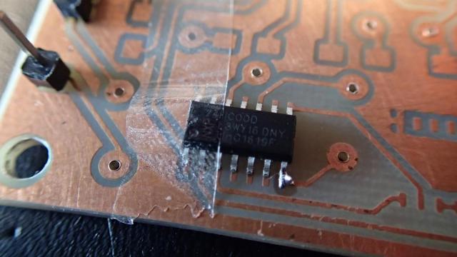
Then I could apply some flux to the remaining pins with a flux pen.
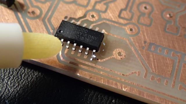
Soldering of the remaining pins was fairly easy. I have used 0.3 mm solder wire and a very thin tip on the soldering iron.
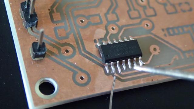
Next I have soldered the pin headers on both sides of the board. The top layer was a bit tricky, but I manage to lift the plastic parts.
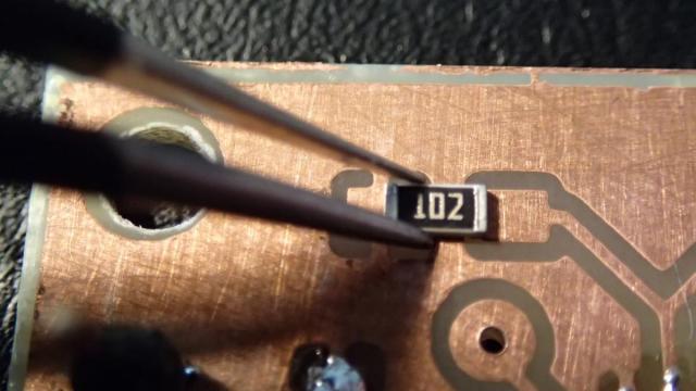
It was time to solder the remaining components. I put them in place using needle nose tweezers.
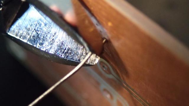
The last thing remaining was to attach the VIAs. I did it by placing a wire though the hole and soldered it on one side. Then cutting it off on the other side with flat cutters and soldered the back side.
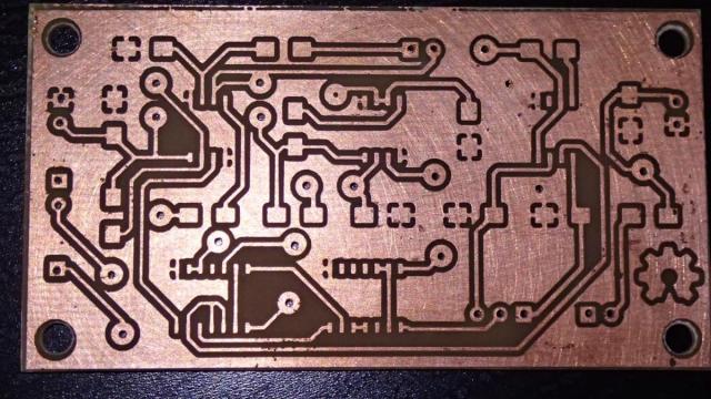
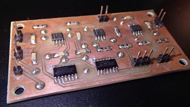
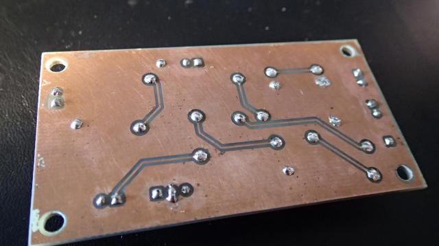
After finishing it, the board looked like this. I made some small mistakes, but for my first board with SMD chips I was happy. Anyway, the absence of a soldering mask does not make it easier.
And the back looked like this:
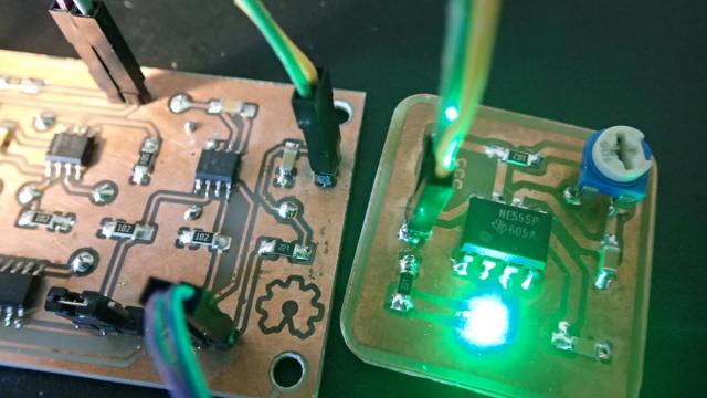
It was time to connect all the external parts and test it. I cheated a bit and used a jumper switch to enable the clock in a-stable mode. It worked the first time! I was amazed!

Then I connected the power pass though to my previousy made board. It worked as well.
It's also nice to see the huge difference in size between the NE555 in DIP and SOIC-8 packages.