In my previous blog post, I demonstrated how I have built this Commodore 64 PLA chip replacement. However it worked fine on my C64 board revision, some of my friends on Twitter tested this chip inside their C64 machines and there were some boards where it did not function at all. In this blog post, I am going to dive a bit deeper into the PLA chip, investigate the reason why it does not work in all C64 machines and then try to fix it.
You can also watch a video version of this blog post:
This blog post is sponsored by PCBWay, which makes very high-quality boards. You just need to upload your design in Gerber files on their website and before you know it they will be manufactured and delivered to your doorstep.
First I wanted to make a circuit that will test the logic of the PLA chip, just to make sure that there aren't any mistakes in the translation of the inputs to the outputs. Then use that circuit and a logic analyzer to measure the delays that are triggered inside the chip, try to fix it and then finally test it.
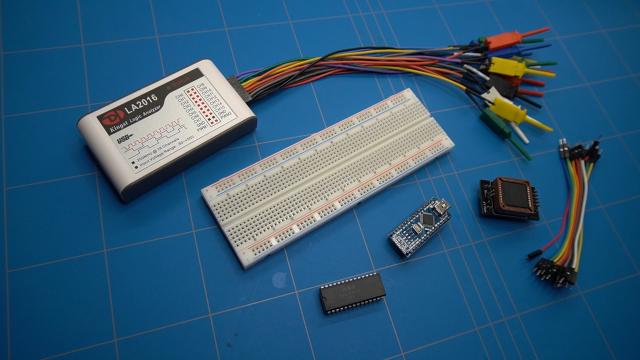
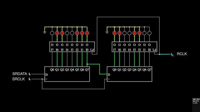
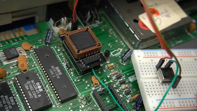
I have gathered all the components that I thought would be needed for an Arduino PLA chip tester. My first impulse was just to stick the PLA chip and an Arduino Nano into the breadboard and connect all the inputs and outputs of the PLA to the Arduino pins until I quickly realized that there are not enough pins on the Nano as we will need at least 24 I/O pins to do the job. So I have decided to use this 74HC595 chip, which has an 8-bit shift register with latch capabilities that will let us shift in serial data using just one of the Arduino pins and convert it to parallel output. When we use 2 of these chips we can address all of the 16 inputs of the PLA chip simultaneously.
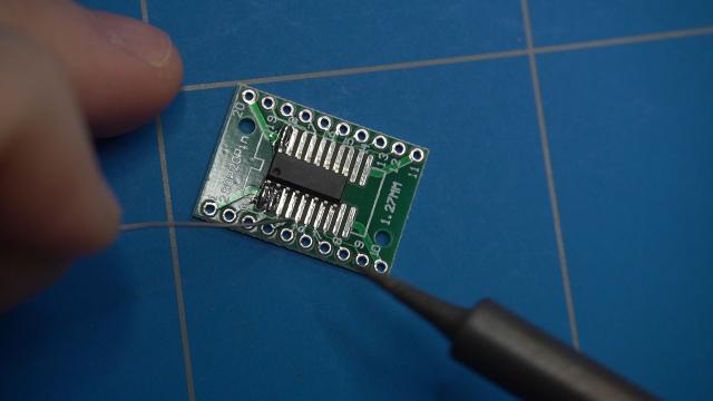
As I didn't have a version of these chips that fit into my breadboard I had to solder it to a PCB which is capable of holding up to 20 pin SOP packages with pin headers.
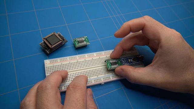
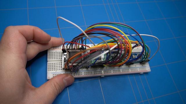
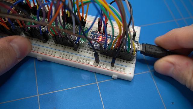
Now it was just a matter of sticking the Arduino Nano, two of the 74HC595 chips and my PLA replacement chip into the breadboard.
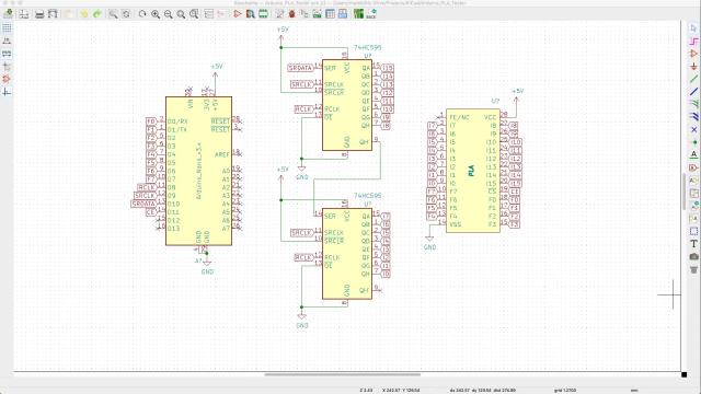
To design the schematics I have used KiCad. Let me hook up the breadboard and explain how it works. First, we will connect the ground from the Arduino to the shift register chips and the ezPLA. The brown wires will connect the output enable of the 74HC595 chip so it will always stay on. The data will be output immediately after we toggle the latch output pin. We will also need 5 volts, which we will tap from the Arduino Nano. The reset pin of the latched shift register will also be connected to 5 volts, as we will never need to trigger it. The green wires connect to the D10 output of the Arduino and as I will show later, it will trigger the storage register clock. These wires connect to the D11 output of the Arduino and will toggle the shift register clock of the 74HC595 chip. Arduino output D12 will be used to program data values into the register. The 2 shift register chips need to be chained together. So the Serial Data output (PIN 9) will connect to the Serial Data input (PIN 14) of the other chip. I am connecting them using these yellow wires. The parallel outputs Qa - through - Qh of both chips need to be connected to the PLA inputs I0 through I15. To test if the outputs of the ezPLA will give correct values I will connect them to the Arduino inputs D2 through D9. Pins D0 and D1 are used for serial communication and programming the chip, so it's better to leave them unconnected.
Before we proceed with the creation of the Arduino sketch that will do ezPLA logic tests, let's have a look at this PDF document called C64 PLA Dissected. Here, the whole PLA chip is analyzed by using die photographs of a real PLA chip. It contains a full logic table that can be used to create logic tests. I have copied this table to a text editor and aligned it a bit to be able to create an array inside the Arduino IDE.
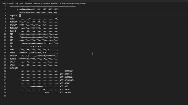
PLA inputs that are set to logic 1 are marked with stars and logic 0 is represented with a slash. A dot basically means that it doesn't matter what value you input.
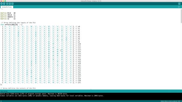
Inside the Arduino IDE, this array represents the same. It is rotated by 90 degrees and I made it a bit more readable by replacing the stars with 1s, slashes with 0s and the dot values with X-es. I did the same for the outputs. Note that the CASRAM table is the only value that is inverted.
Before I will show you the code, let me demonstrate a simulation of how the two 74HC595 chips work as this will help in understanding the Arduino code. What I have drawn here is the internal representation of the 2 chips interconnected to each other. Internally the chip contains a shift register and a latch. When the Shift Register Clock transits from low to high, whatever is on the Data pin will be pushed inside that register. After the 8th pulse, the Q7 output will be passed to the data input of the second chip, so a total of 16 bits can be programmed. After we toggle the storage register clock the contents of the shift registers will be stored on the latch. You can see the contents as they are indicated by the red LEDs. In our case, we will use these outputs and connect them to the inputs of the ezPLA chip.
Let's quickly go through the code. The code can be downloaded from this Github repository.
After defining the arrays for inputs and expected outputs we are setting things up for the 74HC595 chip. Like the register and shift clocks, serial data input, chip enable and the Arduino inputs that will receive data from the PLA chip (lines 82-85). All the magic happens inside the loop function.
In the beginning, we have a for loop that iterates through all of the test cases (line 104). We start the cycle by disabling the PLA chip and setting the chip enable pin to HIGH (line 107). This way we can set all of its inputs and it will not output anything until we pull this signal back to low.
Now we need to set the register clock of the 74HC595 chips to LOW (line 111) to make sure that the output of the storage register will be disabled. I am also printing the test case number we are currently processing (lines 113-116).
And this String variable (line 118) will help us with the processing of what is happening in the second for loop. Here we will push all of the values from the current test case into the shift register (lines 121-153). Just like in the simulation we first need to set the shift register clock pin that is D11 to LOW (line 124). Then we set the data bit according to the contents of the array on D12. If it's a 1 or s 0 inside the array we do a digitalWrite with that value. If it's an X, then it actually does not matter what we set, but I have chosen to set the value of TRUE. The value of the actualTestcase string variable is updated with these values (lines 127-140).
After that, we do a short delay of 50 microseconds (line 145) and set the shift register clock on D11 to HIGH as the value of SRDATA should be shifted on the rising clock pulse (line 149). We wait again for 50 microseconds (line 152) and repeat the cycle for all of the 16 values of the test case.
At this point, all of the data values are shifted inside the shift registers of both chips. Now we can store them on the latch and this will output the values immediately to the inputs of the ezPLA chip as we have wired the output enable of the 74HC595 chips to ground.
We do that by first setting the shift register clock on D11 to LOW (line 16). And this is just to finish the shift register clock cycle. Then we set the Storage register clock on D10 to HIGH (line 166). Now the chip enable pin of the ezPLA can be set to LOW (line 169) and this will allow it to read all the input values. We do a short pause (line 178) and set the storage register clock on D10 to LOW (line 175), which will end the cycle of the storage register.
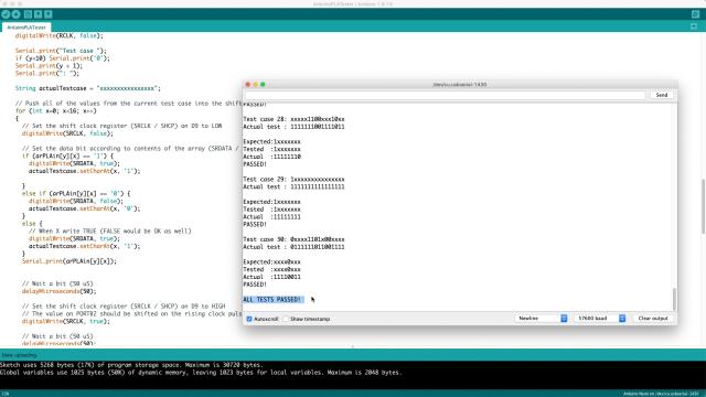
Now we can test the values that ezPLA will output after it has received all of the inputs from the test case. Again we are creating some string variables that will help compare the test results (lines 180-182). The first variable (lines 185-187) is what we expect and it is a copy of the output array that is defined above. Then we read the Arduino pins which contain the data of the ezPLA outputs and store them inside the tested variable. When there is a value of X it is added to the tested variable. The actual string variable stores only zeros and ones (lines 190-200).
The expected and tested variables are compared and if they are equal then the test case passes, otherwise, it fails (lines 209-215). Failed test cases are counted (line 214) and shown in the final output if any tests failed (lines 223-226). Finally, we disable the PLA by setting the Chip Enable pin to HIGH (line 231). And end with an infinite loop (line 234).
This code is specially designed to test the logic of the PLA chip, but it can easily be changed to test other kinds of chips that use a logic table.
Let's connect the Arduino to the computer, upload the code and see what happens.
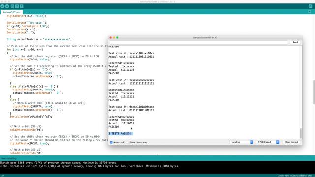
And 3 of the tests have failed! But is the chip faulty or is there a problem with some connections on the breadboard? Could I have made a mistake by misplacing the wires on the breadboard?
There it is! This wire should go here.. and that one over there!
Let's try it now. And this time all tests passed! That means that the truth tables are correctly implemented.
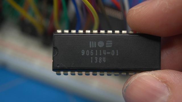
But will this also work on an original PLA? Let's replace the ezPLA with this PLA that I pulled out of a working Commodore 64. Attach the USB to monitor the results and... Luckily this also works.
But somehow the ezPLA does not work on all C64 revision boards. Let's dive back into the PLA dissected PDF.
On page 20 there is a mention that the #CASRAM signal must be delayed by the PLA by at least a certain time. As the #CAS signal from the VIC-II is also used to multiplex the address bus for the DRAM address inputs. This is done with U13 and U25 (74LS257), which have a maximum propagation delay from their select input (#CASRAM) to their outputs of 24 ns. Typical DRAM chips used in the C64 have an address setup time of at least 0 ns before #CAS, an example is the HM4864A ([Hita4846]). This means that the #CASRAM signal must be delayed by at least this time, otherwise, the DRAMs would latch the wrong column address. This timing dependency could be called a design flaw in the C64. The multiplexed address changes about 15 ns after #CAS and becomes stable just about 10 ns before #CASRAM gets active on this board.
To investigate this problem I have attached a logic analyzer to the outputs of the PLA. I am also attaching 1 of the inputs in order to measure the delay. This setup still has the original C64 PLA connected.
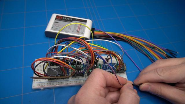
Also, the chip enable pin, that outputs directly from the Arduino, is connected to one of the inputs of the logic analyzer. Let's connect the USB cable to the logic analyzer. We are now inside the logic analyzer software. On the left you can see all of the outputs F0 through F7, the chip enable pin and the last is the A13 input.
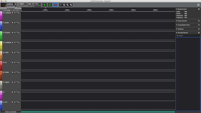
We can now capture the whole test sequence. 5 seconds of data should be enough. It gives me time to trigger the reset button on the Arduino. Let's find the beginning where the input is being triggered and set some markers to measure the delay between input and output of the Original PLA.
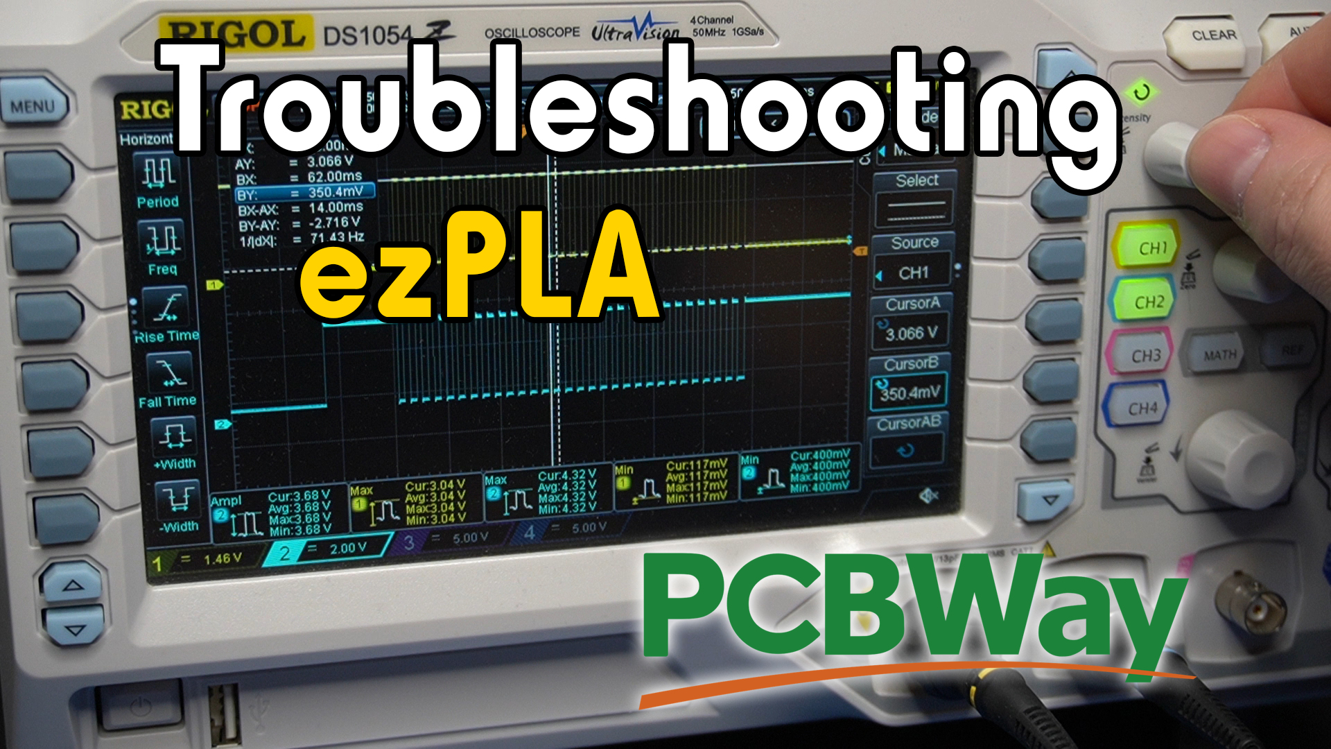
We can see that it is around 30ns. The speed of this logic analyzer is 200MHz which gives a precision of 5 ns, but that should be enough.
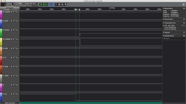
Let's replace the Original PLA with ezPLA and capture the sequence again. After we zoom in, we see that the delay is now. 5ns. This certainly explains when the ezPLA was not working on some Commodore 64 revision boards. I am actually surprised that it worked at all. Maybe it had to do with higher switching speeds of the chips that were used on some C64 boards.
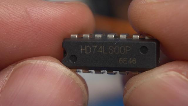
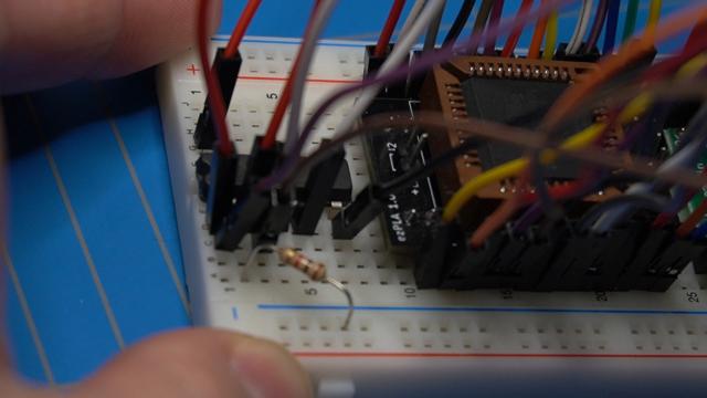
To delay the signal I will use the 74LS00 chip which has 4 NAND gates, simply because I have a couple of them lying around.
According to the 74LS00 datasheet (page 2), the transition from low to high and high to low is between 3 and 15 ns. So my idea is to chain 2 NAND gates together to get this delay. I will not delay all of the output pins, as according to the PLA dissected document, only the CASRAM output delay matters.
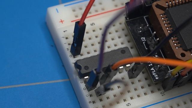
Let's insert the NAND chip and wire it up so the signal of the CASRAM output will go through just one NAND gate. It will be inverted, but this way I can see if this method will work at all.
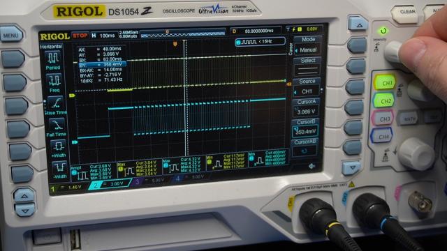
After hooking up the outputs to the logic analyser and capturing the sequence, I noticed that the CASRAM signal was always HIGH, but why is that? Then I connected the output to the scope so I could see exactly what was happening and I found out that the signal was toggling between 1.3 and 3.7 volts.
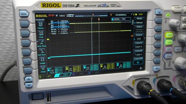
When we look at the datasheet of the 74LS00 chip it shows that the low signal needs to be lower than 0.8 Volts and because the output of the NAND gate was at 1.3 volts it could never see the LOW output signal. And was always high. To fix this, I have added a 1K pull-down resistor from the output to the ground, which should lower the LOW output signal of the NAND gate. And when we look at the scope, we can see that the LOW signal is now at 350 millivolts, which should be low enough to trigger the logical 0.
Now I could wire up the CASRAM signal to the second NAND gate and see if it will work.
After capturing the sequence, we can see that it works now. So let's zoom in and see the delay that is now on the signal. We now have 10ns of delay more than the other output signals have.
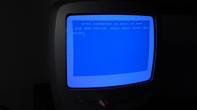
Let's see if it's enough by hooking up another breadboard with just the ezPLA on it with the delay chip. My method is a bit awkward, but I have managed to connect it to the PLA socket.
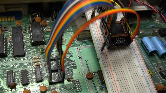
Moment of truth... and? It works!
I will still need to change the ezPLA PCB that shall include the 74LS00 chip and the pull-down resistor, but this is a matter for the next blog post.
I have also tried to change the delay of the chip by using a crystal oscillator and by changing the VHDL code, but I could not make it work on a breadboard as the speed of the crystal was 32MHz. I might create another version of a PCB with the crystal in place and try this again.
But for now, that's it. I hope that you learned something new and I hope to hear from you in the future.