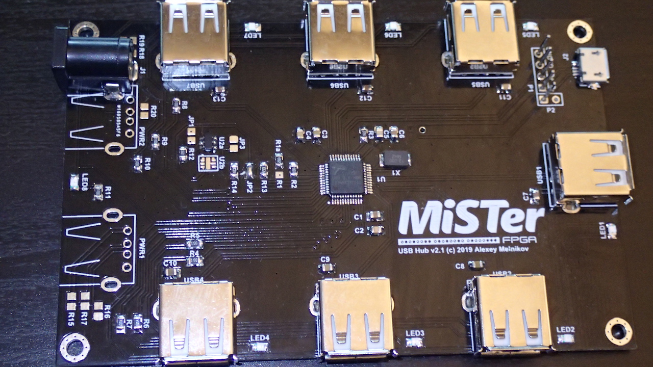
When you need to connect more then one USB device to your DE10-Nano FPGA board then you need to use a powered USB hub. It is possible to use normal hub, but it is way cooler to connect the one that is custom designed for the MiSTer project.
Watch the full video tutorial on youtube:
To start with you will need the MiSTer USB Hub 2.1 boards. You can easily order them with one click on PCBWay.
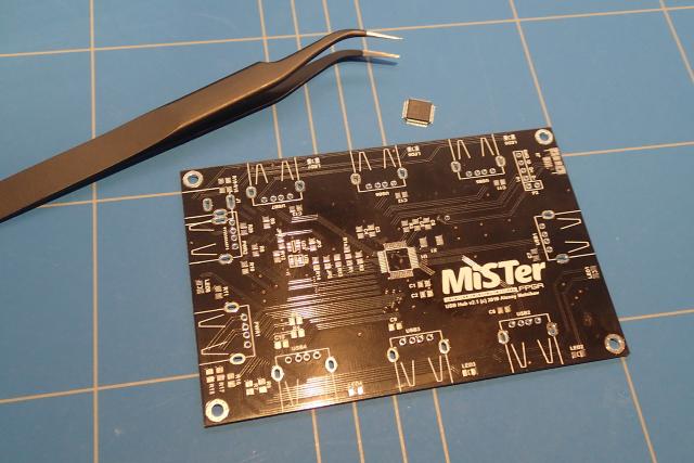
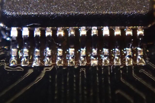
First step in the assembly the PCB is to solder the FE2.1 USB 2.0 7-port hub controller chip. This is the heart of the USB Hub. Make sure you have needle tweezers as they will help you with positioning of the chip and later with placement of the SMD components.
To place the chip I always use transparent adhesive tape and stick it to the PCB. It is a delicate procedure so arm yourself with patience. Make sure you have aligned all 4 sides of the chip.
Now you can solder the corner pins, so it will stay in place when you drag solder the remaining pins.
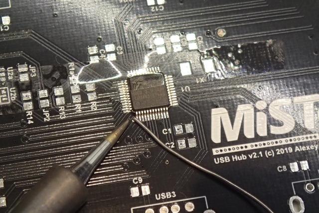
Make sure you apply enough flux for this step. I use gel flux, but you can also use a pen which has flux in more liquid form.
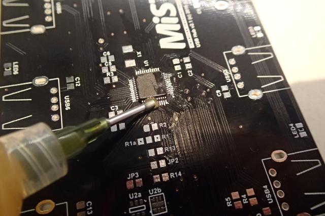
Now you can drag solder the remaining pins. There are also a lot of youtube tutorials on how to do drag soldering. Make sure to check them out.
If you make bridges between the pins you can clean them out using desoldering wick.
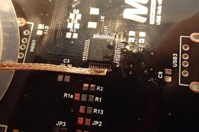
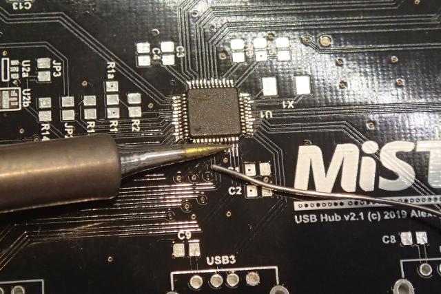
After you are finished use isopropyl alcohol (IPA) to clean up the remaining flux.
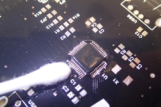
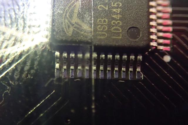
The pads of the chip should end up looking like this.
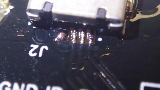
The next component that I have soldered was the micro-USB connector. This can be done in a similar way as the FE2.1 chip. Using clear adhesive tape to hold it in place and then tick soldering all the pins. Make sure to add enough solder and heat on the sides of the connector so it will not fall off when you try to insert the USB plug. (Never happened to me...)
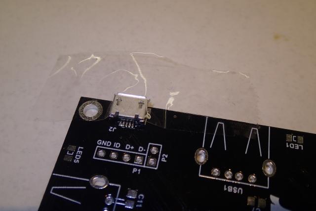
The connector should look like this. (It is ok to bridge the 2 pins as shown on the picture)
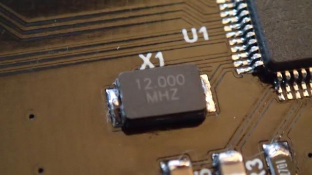
To solder the 12 MHz crystal you need to apply some solder on the PCB pads as this components has soldering pins that are under and don't stick out much to the sides. Use enough heat of your soldering iron while holding it with needle tweezers to solder it firmly.
There is another chip on the board U2 (which is optional). It is responsible for current limiting on the board. You have a choice between U2a and U2b, which are NCP380LSNAJAAT1G and NCP380LMUAJAATBG respectively. I have chosen for U2a as the TSOP6 package is a bit easier to solder.
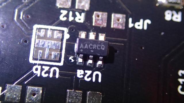
In the MiSTer USB Hub 2.1 schematics there are some guidelines on what components to solder / not to solder when you are using this chip.
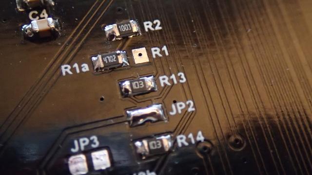
However there is no mention about soldering R1a instead of R1. This is needed, otherwise you will be drawing current directly from USB and not the power supply. To bridge the JP2 jumper you can use a blog of tin.
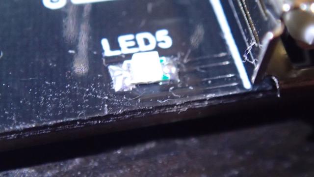
Now you can solder the 8 LEDs. 7 are green for the USB ports and the 7th (red) is for power.
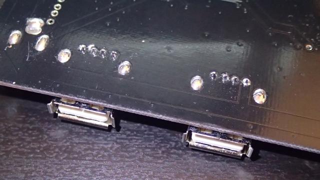
Next you can continue to solder the USB ports. I have setup the temperature of the soldering iron a bit higher, as the ground pins are in direct connection to the metal chassis of the USB connectors.
One of the last things to solder on the board is the 5V barrel power connector.
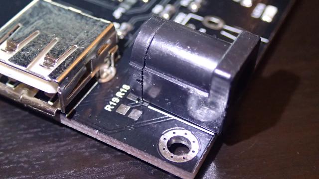
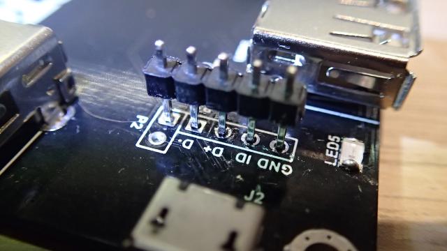
To connect the USB Bridge to the DE10-Nano board you need to solder some header pins. After you have finished with soldering, lift and remove the plastic part. If you don't do this, the USB Bridge will not fit under the FPGA board.
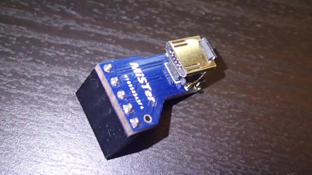
To finish, solder the USB bracket board. I have used the one for L-shaped USB connector that is called USB Bracket 2.1 inside the GIT repository. It looks like this
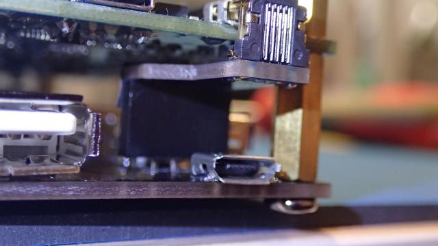
Connect the USB bridge to the DE10-Nano board in this way:
Please contact me if you have any questions or run in trouble when soldering. You can also buy one that is fully soldered and tested in my Tindie store.