The basic building blocks of FPGA chips are logic elements (LEs). A logic element consists of LUTs (look-up tables), which are basically programmable logic gates. This gate is a multiplexer and can be build out of NAND gates. This small project is a breadboard implementation of this concept.
A LUT is basically a 4-to-1 multiplexer. It is possible to implement any logic function using this small block.
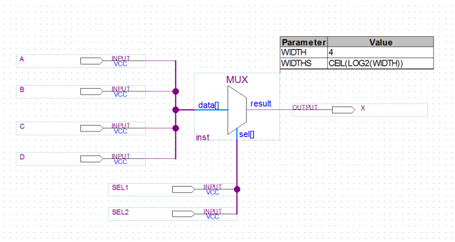
To choose from 4 possibilities (A through D) we need 2 inputs (SEL1 and SEL2). The output of this decoded selection is X. If we make a table of all possible selections related to output it would look like this:
| SEL1 | SEL2 | X |
|---|---|---|
| 0 | 0 | A |
| 0 | 1 | B |
| 1 | 0 | C |
| 1 | 1 | D |
Now imaging we connect A,B,C to 0 and D to 1, we will get the truth table of an AND gate. When we make A equal to 0 and B,C,D to 1 we get an OR gate.
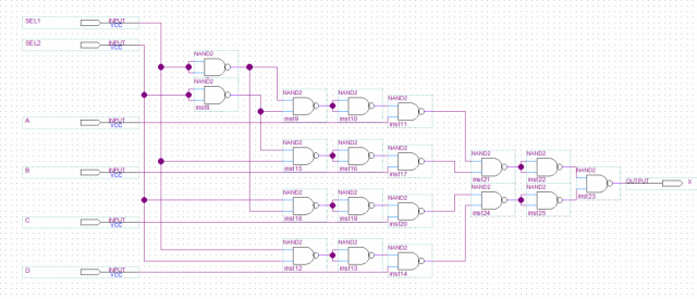
In order to build our multiplexer, we can use logical gates. For this purpose we are using NAND3, 4 and NOT gates. Below you can see the schematic.
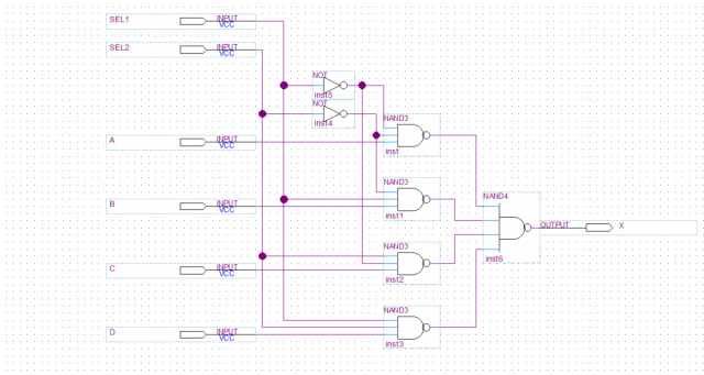
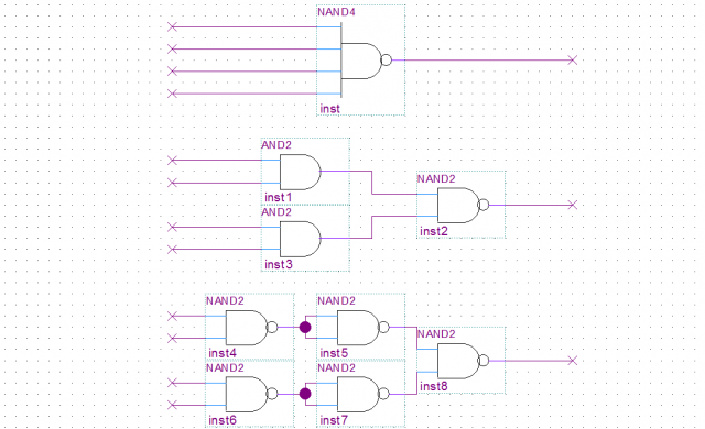
In this project I have decided to only use NAND gates as they are kind of LEGO system of logic. The other advantage is that we will just need one type of chip, namely the 74LS00. This chip has 4 integrated NAND gates and they all have 2 inputs. So it is required to transform the NAND with 3 inputs to NAND gates with 2 inputs. Below are the steps on how to accomplish this.
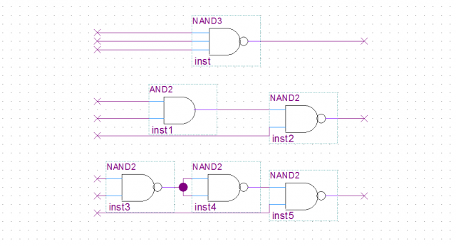
The same applies for the NAND gate with 4 inputs.
I left out the diagram of the conversion of NOT gate to NAND as you can see it in inst5 and inst7 in the schematic above.
Eventually we will end up with this design:
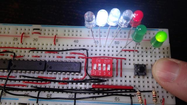
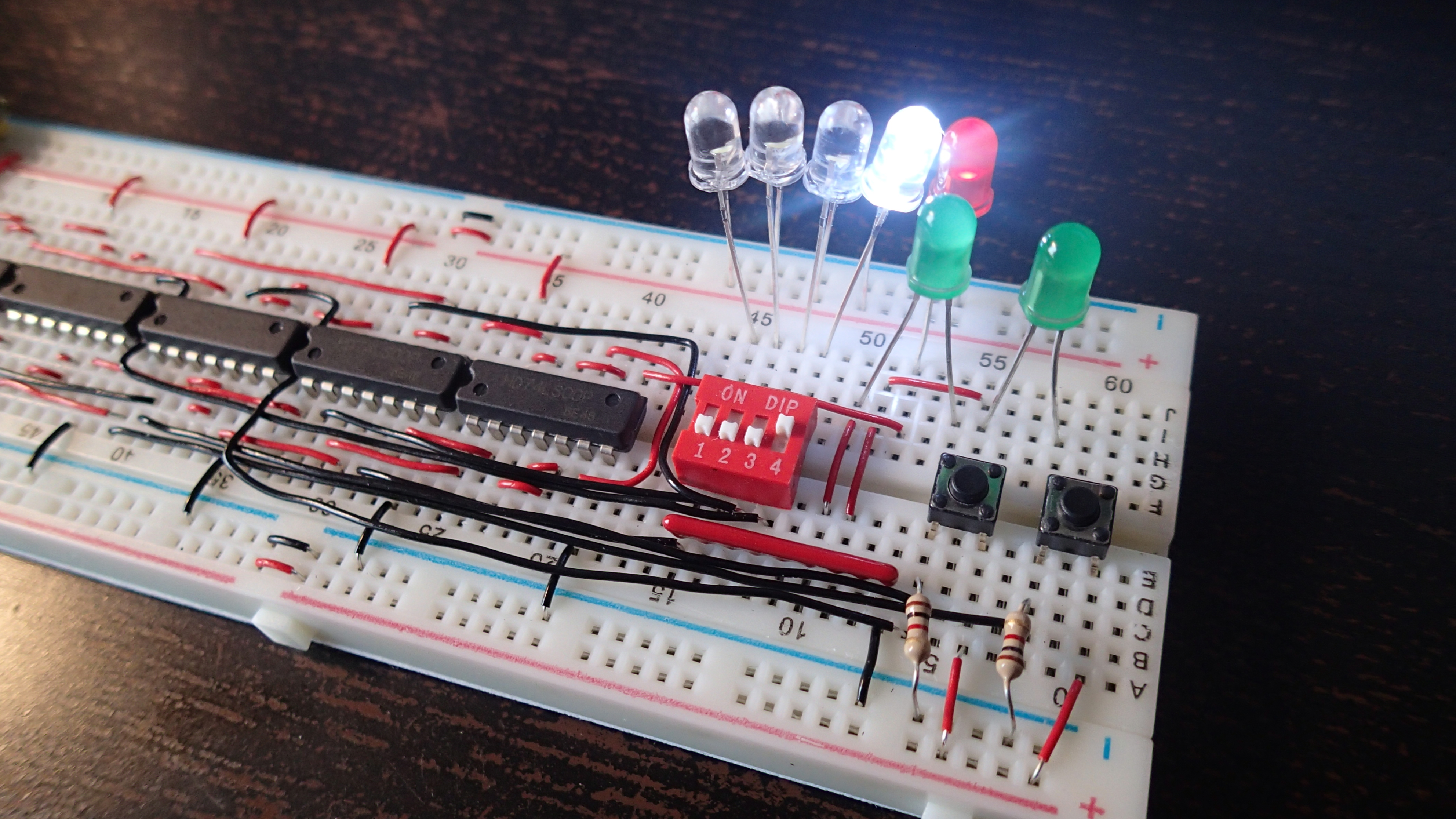
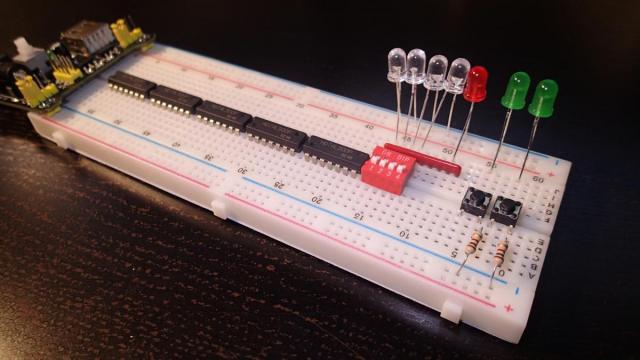
It is time to inventorize which part are needed to implement this design on a breadboard. Since there are 19 NAND gates and there are 4 gates in a 74LS00 chip we will need 5 of them. We will also need some kind of memory to store our A through D values. In real FPGAs SRAM memory is used, but in our case a simple 4 way DIP switch will suffice. Also 2 input switches to emulate our selection values, some LEDs as indicators and resistors for current limiting of the LEDs and pull-down for our switches. In my case I am using a 330Ohm resistor network and 2x 1KOhm resistors. Not to forget a 5V power source, breadboard and some wire to make our connections.
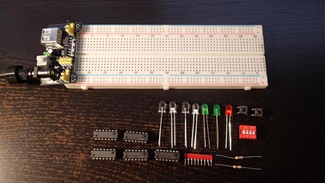
I have placed the components on the breadboard, some of them will swap location during the routing of the wires.
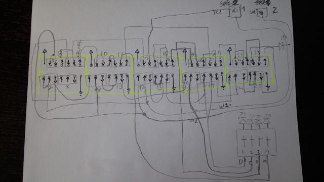
While connecting all the pieces on the breadboard I was keeping progress on a simple piece of paper. It was a pretty chaotic, but in the end it all worked out.
After a couple of hours of this therapeutic exercise the breadboard was finished. For a change it worked the first I powered on the circuit.
The example below shows the implementation of an XOR gate. This wiki page about logic gates show some more examples with truth tables.