FPGA's and CPLD's are certainly very cool devices. It is possible to create you own logical circuits and emulate real hardware chips on the lowest level. For this test project we will use Alera CPLD which is also known as MAX3000A and it's full code is ALTERA EPM3064ATC44-10. It has a programming capacity of 64 macrocells. A macrocell is the smallest programmable part inside a CPLD. The capacity of 64 is not very large compared for example to Altera Cyclone IV EP4CE6E22C8N FPGA chip which has 6272 logical elements, but it will be suitable for small projects. Certainly enough to create a blinking led.
We will be using Quartus II 13.0.1 Webedition version, which is a free IDE to develop and test your projects. The correct version is important, as it needs to support our MAX3000 device.
To program your Altera device you will need a JTAG programmer as USB Blaster. In this blog I will not cover how to do a full set up or this JTAG programmer, there are plenty of tutorials online. I will only focus on the block diagram and the VHDL code to blink the led.
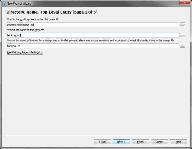
First we will need to create a new project in Quartus. This can be done by selecting the New Project Wizard in File menu. Specify the directory for your project and the name. In our case it will be blinking_led.
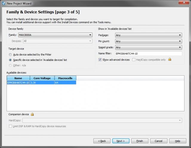
Click next in the step 2 of the wizard and in step 3 select Device family MAX3000A. In the Name filter you need to type in: EPM3064ATC44-10. You will see that this device is powered by 3.3V. Click on Finish and your project will be created.
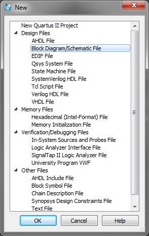
Create a new file which is of type Block Diagram/Schematic file.
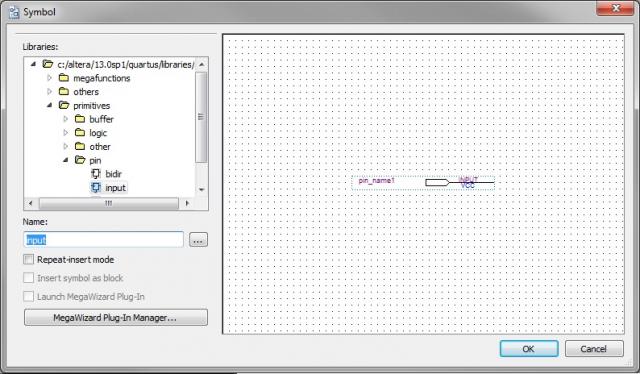
Double click on the canvas and this will pop-up a dialog where you can insert a input and a output pin.
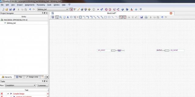
This is how it will look after you have completed the step above. Click ctrl-s (or select File -> Save in the menu). Safe the file as blinking_led.bdf. The program should already suggest that name. Note that it is important to name this file the same as your project, otherwise you will get compiling errors.
Now create a new file and this time select VHDL file. You will get an empty editor window. Paste in the code from below and save the file again as something like clock.vhd. The variable tick will determine how fast your led will blink.
library IEEE;
use IEEE.std_logic_1164.all;
use IEEE.numeric_std.all;

entity slow_clock is
  port (
    sysclk: in std_logic;
    clk_out: out std_logic
  );
end entity slow_clock;

architecture ar_clock of slow_clock is
  signal led_state: std_logic := '0';
begin

  clock : process(sysclk)
    variable tick : integer := 25000000;
    variable count_clk : integer range 0 to tick;
    begin
      if (rising_edge(sysclk)) then
        if (count_clk = tick) then
          count_clk := 0;
          led_state <= not led_state;
        else
          count_clk := count_clk + 1;
        end if;
      end if;
  end process clock;

  clk_out <= led_state;
end architecture;
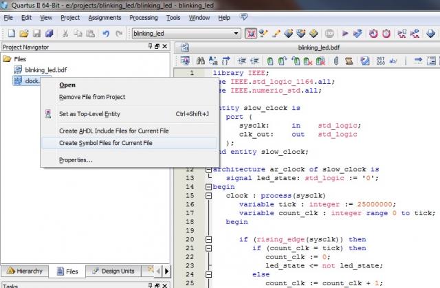
Now switch to Files tab (next to the Hierarchy tab in the Project Navigator window) and right click on the clock.vhd file and select Create Symbol Files for Current File. This step is important as it will allow you to add a block diagram of our created clock.
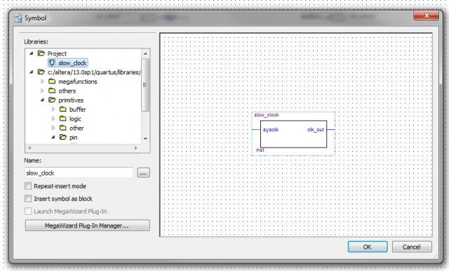
Now close he compilation report tab, go back to your blinking_led.bdf (block diagram file) and double click on the canvas. In the Libraries you will see a new group Project and a new schematic which is called show_clock. Insert it in your block diagram by clicking OK.
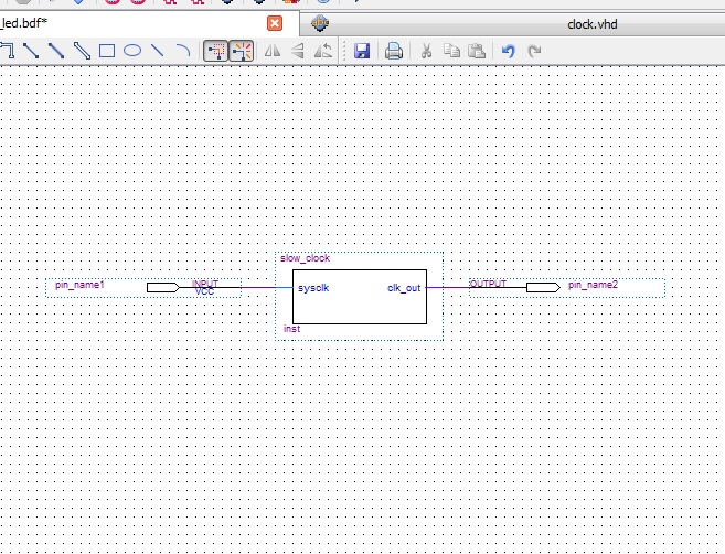
Now place it on the canvas and connect the sysclk to the input pin and the clk_out to the output pin. Just like in the screenshot below.
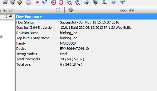
Now start the compilation of the project. (Processing -> Start Compilation or press Ctrl+L). Save any changes if prompted. The compilation should be successful (with some warnings that can be safely ignored).
The compilation window will show that we have used 59% of the total of all microcells. You can also see that we have used 6 of 34 pins. You may think that this is not true, because we have only used 2. But actually the 4 other pins are reserved for the JTAG programmer.
They are:
- TDI (Test Data In)
- TDO (Test Data Out)
- TCK (Test Clock)
- TMS (Test Mode Select)
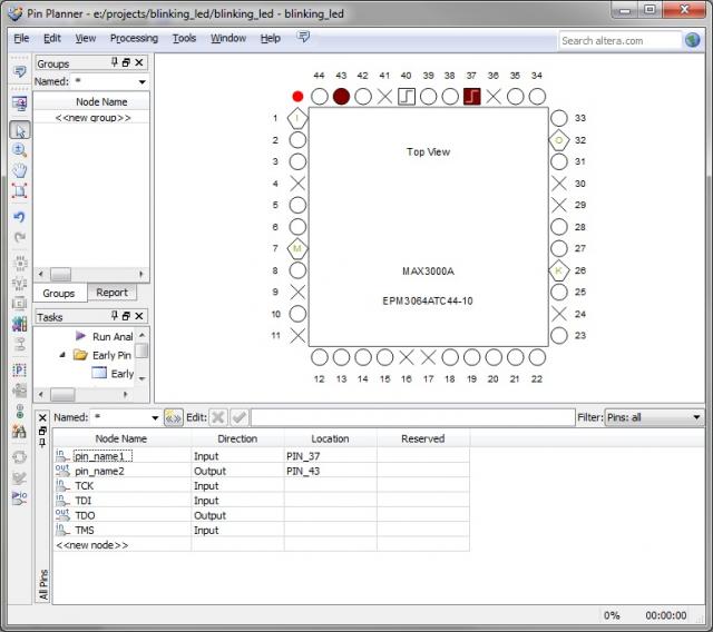
Now it's time to open the Pin Planner dialog and assign the input and output pins from to physical pin on the chip. This is done by clicking on the Pin Planner icon (or menu Assignments -> Pin planner).
Here you can select pin_name1 (which is our input pin) and assign it to the global clock pin which in our case is PIN_37. The LED on our board is connected to PIN_43, so we select the Location of pin_name2 to this pin.
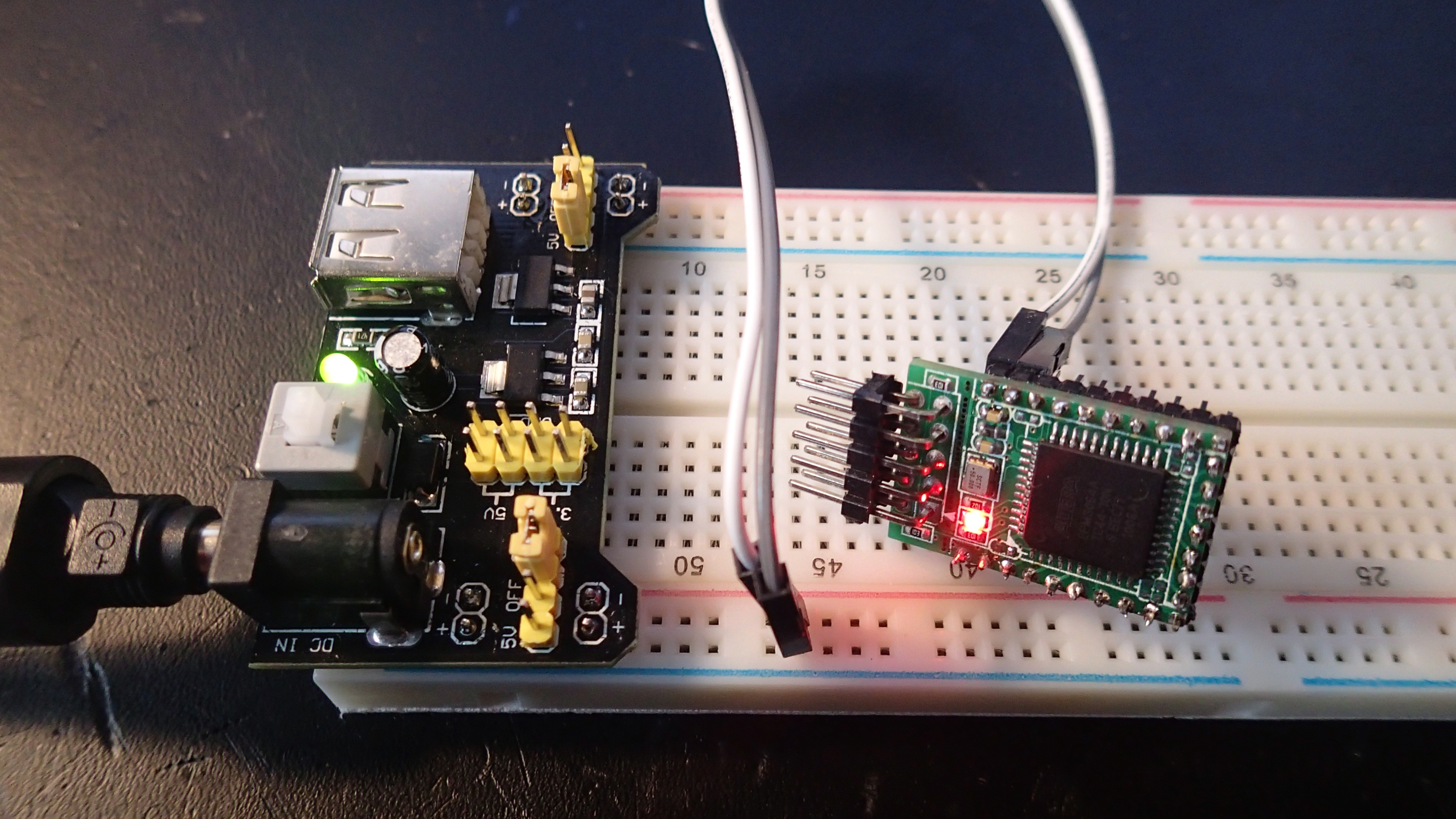
Now we are going to connect our board to the JTAG programmer and power supply. The JTAG cable does not supply power so we need to provide it from an external source. Without power the board will not program.
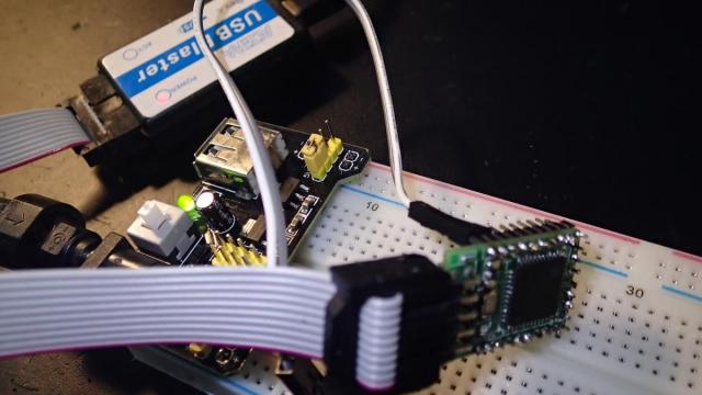
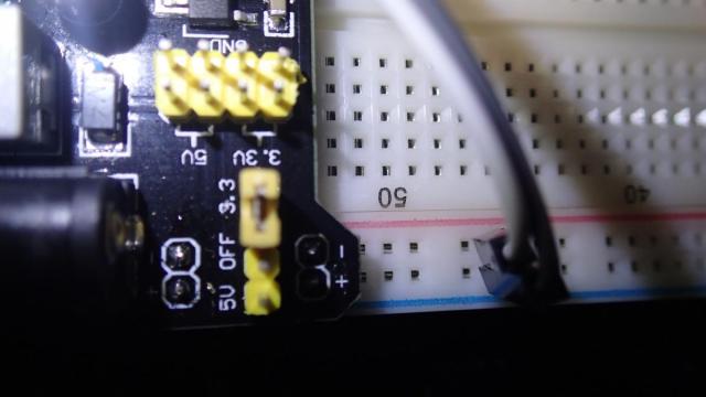
I am using this breadboard power supply which has 3.3V option simply be setting the correct jumpers.
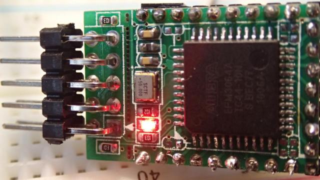
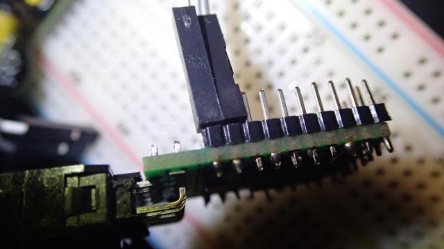
On the CPLD board supply the power to those 2 pins in the corner. I have used a multi-meter to pinpoint the correct ones. Ground is in the corner pin and +3.3V is just below it. I could not prick in into the breadboard, because the DIP spacing is different (2.0mm), so this is the reason for the 2 wires.
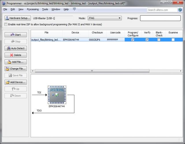
It is time to finalize our project. First we will re-compile it and then go the Programmer dialog, which is located in Tools menu. In this dialog make sure that you have selected the correct JTAG programmer. In my case it is USB-Blaster. Then select the Program/Configure and Verify check-boxes. If you press the [Start] button it will program the EEPROM memory of the CPLD chip.
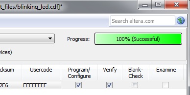
You should get a green 100% bar and the led on your board should start blinking.
I hope this small test project will encourage you to play around with FPGA and CPLD devices. If you have any questions don't hesitate to contact me.